
1 Introduction
With the continuous advancement of technology, the wired connection method in most fields can no longer meet the requirements of high-speed development of science and technology. Wireless communication is entering various fields in our life. Compared with wired connection, it is portable and flexible. Do not have to consider the advantages of routing. It has a wide range of applications in wireless alarm, industrial data acquisition, remote control, telemetry RF IC card, handheld PDA, wireless image transmission, non-stop charging, wireless meter reading and other aspects. The temperature measurement system described in this paper is also one of the applications of wireless communication systems. It uses SOC MCU C8051F020 as the central controller, and CC1000 as the wireless transmission module and temperature measurement circuit to form a multi-channel wireless temperature acquisition system.
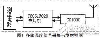
Collect 8 channels of temperature data and send them to the host C8051F020 for processing.
The modulation and demodulation is completed by CC1000. The system adopts frequency shift keying modulation (FSK), the carrier frequency is 433MHz, the bandwidth is 64kHz, the data is transmitted by differential Manchester coding, and the air transmission data rate can be set as needed. At the time of transmission, the controller C8051F020 receives the acquisition command from the user interface, collects 8 temperature signals, and converts the collected temperature data into data frames for transmission to CC1000, and controls CC1000 for data transmission.
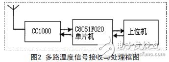
At the time of reception, the controller C8051F020 receives the temperature data transmitted from the CC1000, performs simple processing, and transmits the data to the host computer for detailed analysis processing. The hardware block diagram is shown in Figure 1 and Figure 2.
2. System hardware design
2.1 Wireless transceiver module
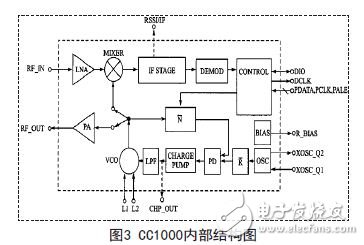
The wireless transceiver module of this design adopts the high-performance RF transceiver chip CC1000 of ChipconComponent. It is a single-chip high-frequency wireless transceiver IC with low current consumption and adjustable communication rate up to 72.8kbit/s. The receiving sensitivity is -109dB.m, the transmit signal power is adjustable within -20~10dB.m. The design circuit is simple, the peripheral components used are few, the coding is simple, and the circuit and device parameters can be changed to make the frequency range of 300~1000MHz. Internal change. At the same time, the device integrates a transmitting power amplifier, FSK modulation/demodulation, low noise receiving amplifier, mixer, voltage controlled oscillator, phase detector and other circuits. It is a highly integrated chip that can directly communicate with the microcontroller. Communicate. The IC is very suitable for embedding into various measurement or control systems with high power consumption requirements. We select the 433MHz frequency band in this system. The CC1000 internal structure diagram is shown in Figure 3.
2.2 main control chip C8051F020 and control circuit
C8051Fxxx is a series of 8-bit high-speed system-on-a-chip (SOC) microcontrollers from Cygnal. The C8051F020 is one of them. Its CIP-51 is fully compatible with the MCS-51 instruction set. It has the following advantages: (1) high speed, maximum The processing speed can reach 25MIPS; it fully meets the real-time requirements in this design. (2) High integration, on-chip integration of extremely rich analog and digital peripherals: two multi-channel analog-to-digital conversion systems, including an 8-bit ADC and a 12-bit ADC, and two programmable gain amplifiers and two An analog multiplexer; two 12-bit/analog conversion systems; two analog comparators: an on-chip temperature sensor; a rich bus interface including an SMBus bus interface, a universal asynchronous serial bus interface UART, and an SPI bus interface; Five 16-bit general-purpose timers; eight 8-bit I/O ports; one 64K FLASH and one 256B internal RAM one 4096B external RAM (XRAM); and watchdog circuits; these on-chip resources are greatly reduced The hardware circuit design of this design greatly shortens the development cycle. (3) The crossbar makes the I/O port assignment more flexible.
Based on the on-chip resources of C8051F020, it can fully meet the real-time acquisition and processing of multi-point temperature data. The control circuit of C8051F020 to CC1000 is shown as in Fig. 4.
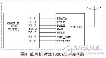
As shown in Figure 4, the microcontroller C8051F020 uses P3.0, P3.1, P3.2 and CC1000 PDATA (program data), PCLK (program clock), PALE (program enable) connection to program configuration and calibration of the CC1000. Operating at 433MHz with a bandwidth of 64kHz, the data is transmitted using differential Manchester encoding. The P0.2 and P0.3 of the MCU C8051F020 are connected with the DIO and DCLK of the CC1000 for data transmission and reception. The MCU packs the collected temperature data to the DIO pin of the CC1000 via the P0.2 pin, and the DIO pin. The input digital signal is frequency-shifted (FSK) and sent to the power amplifier, and then transmitted through the CC1000 antenna; the RF signal received by the CC1000 antenna is amplified by a low-noise amplifier (LNA) and sent to the mixer, and then The demodulator (DEMCO) demodulates into a digital signal and is output by the DIO pin. The P0.2 pin of the MCU receives the digital signal of the DIO pin and transmits it to the host computer for analysis and processing.
The magnetic buzzers (Self-drive Type) offer optimal
sound and performance for all types of audible alert and identification. Our
Magnetic Buzzer solutions are offered with various mounting options. We also
provide you with a washable version for your preferred soldering method. Our magnetic buzzers, also known
as indicators, are designed with an internal drive circuit for easy application
integration. During operation, current is driven through a voice coil to
produce a magnetic field. When a voltage is applied, the coil generates a
magnetic field and then allows the diaphragm to vibrate and produce sound. This
Buzzer type has a low operating voltage ranging from 1.5 – 12V+. Our magnetic
buzzers are desirable for applications requiring a lower sound pressure level
(SPL) and frequency.
Magnetic Buzzer Self-drive Type
Passive Buzzer,Dc Magnetic Buzzer,Electro Magnetic Buzzer,Magnetic Buzzer Self Drive Type
Jiangsu Huawha Electronices Co.,Ltd , https://www.hnbuzzer.com