
1 Introduction
OMR is an optical mark card information input device, widely used in the field test, census, lottery, elections. At present, there are a variety of cursor readers at home and abroad, with complex structure and high production cost. This paper introduces a new type of cursor reader system based on DSP TMS32OF2812. The system has the characteristics of simple structure and low cost, and has strong practical value.
2 hardware structure
The hardware of the cursor reader is generally composed of LED sensor, ADC, data processing control unit, PC interface, paper feeding control, etc. Currently, there are two kinds of hardware structures for optical marking readers commonly used: data processing control unit adopts industrial control board mode and data. The processing control unit adopts the DSP+FlaGA method. These two circuits are more complicated and have higher production costs.
This paper introduces the data processing control unit based on TMS320F2812 hardware structure. TMS320F2812 is the 2000 series digital signal processor developed by American TI company. It is the first one with on-chip Flash and working frequency up to 150 for motor control and industrial automation. MHz 32-bit DSP. TMS320 F2812 adopts the classic Harvard bus structure, which uses multiple buses to convert data between memory, peripheral modules and CPU. This multi-bus structure makes it possible to fetch, read and write data in parallel in one cycle. Instruction pipeline technology ensures fast and real-time signal processing. The internal memory of the TMS320F2812 includes 14 K of RAM and 128 K&TImes; 16 bit of Flash: on-chip integrated 16-channel 12-bit ADC module, 16-channel PWM output, up to 56 independent programmable GPIOs, 3 with 6 The general purpose timer of the mode, three comparators with configurable dead zones, three single-ended comparators, and four capture units. A variety of serial interfaces are also integrated [1].
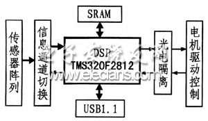
The basic structure of the system is shown in Figure 1, with internal A/D conversion. The TMS320F2812 is the core and the data transmission uses the USB interface. The system has the advantages of simple electrical structure, low cost, fast acquisition and processing speed, and fast data transmission.
3 data collection
The optical marker reader is an optical marker information data acquisition device. Acquisition speed and accuracy are two very important aspects. The acquisition module of this system adopts the internal A/D module of TMS320F2812. This module is a 12-bit analog-to-digital converter with pipeline structure. It has built-in dual sampler (S/H), which can select 16 channels of input and fast conversion time. Run at 25 MHz or 12.5 MHz. The input voltage range is 0 V to 3 V, the single conversion time is 200 ns, and the pipeline conversion mode conversion time is 60 ns. The ADC module has two independent sequencers that can work in the dual sequencer mode and the cascade sort mode [2]. Provides high acquisition speeds.
The internal error of the TMS320F2812 ADC has gain error and offset error, which needs to be corrected. Otherwise, the signal accuracy will be affected. The conversion equation can be expressed as y=x&TImes;ma±b, where ma is the actual gain and b is the offset error. By measuring the ADC signal acquisition of the TMS320F2812, it is found that the ADC gain error is generally within 5%. It can be corrected by the following methods: any two channels of the ADC are selected as reference input channels and respectively provided to their known DC reference. The voltage is used as an input (the two voltages cannot be the same). The conversion value is obtained by reading the corresponding result register. The correction gain and correction offset of the ADC module are obtained by using two sets of input and output values, and then the conversion of the other values ​​is performed by using the two values. The data is compensated to improve the accuracy of the ADC module conversion. The specific calculation process is as follows:
1 Get the converted values ​​yL and yH of the known input reference voltage signal.
2 Calculate the actual gain and offset error using the equation y=x&TImes;ma+b and the known reference values ​​(xL,yL) and (xH,yH): the actual gain ma=(yH-yL)/(xH-XL); Offset error b = yL - xL x ma.
3 Define the input x=y×CalGain-CalOffset, then the correction gain CalGain=1/ma=(xH-xL)/(yH-yL) is obtained by the equation y=x×ma+b, and the correction offset CalOffset=b/ma= yL/ma-xl.
4 Apply the corrected gain and correction offset to other measurement channels to correct the ADC conversion result.
The gain and offset error between the channels of the TMS320F2812 ADC conversion module are all within 0.2%. Therefore, it can be corrected by the above method [3]. The experimental results show that the error of the corrected ADC is controlled within 0.5%, which greatly improves the acquisition accuracy.
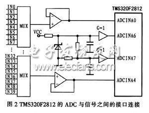
The signal input of the system design is 40 channels, and the ADC input channel of the DSP itself is 16 channels, so an external multiplexer is required for expansion. In the circuit design, five DSP ADC input channels ADCINAO~ADCINA4 are used, and one channel is connected with one 8-input and one-output multi-channel analog converter 4051. Expanded to 40 analog signal inputs. Figure 2 shows the interface between the ADC and the signal of the TMS320F2812.
4 data communication
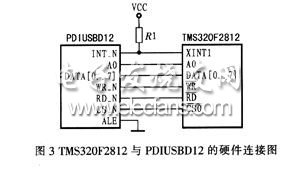
The cursor reader is a fast device that recognizes several information cards in one second and needs fast data transmission between the PC and the PC. The system uses USB communication method and adopts a cost-effective USB device PDIUSBDl2, which is usually used. High-speed communication with the microcontroller in the microcontroller system is fully compliant with the USBl.1 specification. PDIUSBD12 and TMS320F2812 both work at 3 V, they are connected by parallel port, and PDIUSBD12 is assigned a chip select. TMS320F2812 can operate by reading and writing address. PDIUSBDl2 parallel port interface rate is 2 MHz. Compared with TMS320F2812 It belongs to the low-speed device and needs to be set in the software to insert the waiting period. FIG. 3 is a hardware connection diagram of TMS320F2812 and PDILISBI) 12.
For lithium iron phosphate(LiFePO4) power battery system with brand of Taihang Jiaxin, it has the advantages of long cycle life, high rate of discharge performance, good safety, available for the requirement for Fast Charging and so on.
Using self-developed Battery Management System (BMS) which has the functions of advanced battery self-management, communication, alarm and other functions.

Lifepo4 Battery Pack,Lifepo4 Battery Pack 12V,24V Lifepo4 Battery Pack,48V Lifepo4 Battery Pack
Xinxiang Taihang Jiaxin Electric Tech Co., Ltd , https://www.chargers.be