
Evaluation and design support
This article refers to the address: http://
Circuit evaluation board
CN-0263 Circuit Evaluation Board (EVAL-CN0263-EB1Z)
Design and integration files
Schematic, layout file, bill of materials
Circuit function and advantage
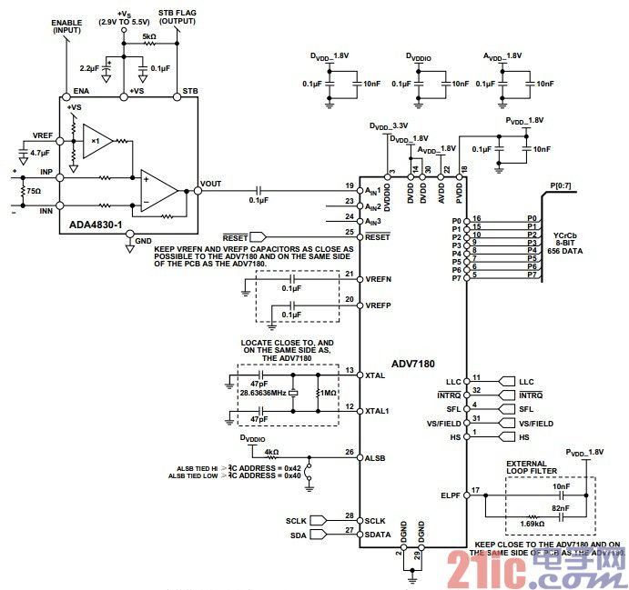
Figure 1. Robust differential video receiver with ADA4830-1 and ADV7180 (all connections and decoupling not shown)
The circuit shown in Figure 1 provides an extremely robust solution with integrated overvoltage (Battery Short Circuit [STB]) protection to receive CVBS video signals in harsh environments. It uses the low-cost, low-power, unipolar, differential receiver ADA4830-1 to convert fully differential or pseudo-differential (ground-referenced single-ended) video signals into single-ended signals before the ADV7180 is digitized.
The ADA4830-1 is used to eliminate common mode noise and phase noise due to the ground potential difference between the input video source and the receiver circuit. More importantly, the combination of the ADA4830-1 and ADV7180 provides very robust input characteristics that can operate in harsh automotive environments, as well as protect and detect battery short-circuit events and meet the stringent requirements of automotive manufacturers.
The robust receiver circuit uses the ADA4830-1 and ADV7180 to conform to traditional, proven isolated/standalone low-voltage integrated circuit architectures such as the ADV7180 from outside and using amplifier circuitry for signal conditioning and protection.
The ADA4830-1 (single channel) is a single-chip high speed differential amplifier that integrates input overvoltage (battery short) protection up to 18 V, providing a wide input common-mode voltage range and excellent ESD robustness. It is designed to be used as a receiver for differential or pseudo differential CVBS and other high speed video signals, suitable for operation in harsh, noisy environments such as automotive infotainment and vision systems.
The ADA4830-1 combines high speed and precision to accurately reproduce CVBS video signals while suppressing unwanted common mode error voltages.
With STB protection/detection, robust ESD tolerance, and a wide input common-mode voltage range, the ADA4830-1 can be used as a vehicle analog video receiver in systems such as rear-view cameras and rear-seat entertainment.
The ADV7180 and ADA4830-1 are fully compliant with automotive applications and are ideal for infotainment systems and visual security systems in automotive applications. The ADV7180 and ADA4830-1 are available in very small LFCSP packages for space-constrained applications.
Circuit description
The ADA4830-1 is a single-chip high speed differential amplifier designed for automotive applications. The design is based on a traditional 4-resistor differential amplifier and is optimized to avoid the errors that are easily made when applying the standard amplifier application circuit.
When an input overvoltage condition is detected, the battery short-circuit protection integrated into the ADA4830-1 utilizes a fast switching circuit to clamp and maintain the internal voltage node at a safe level. This protection allows the input of the ADA4830-1 to be directly connected to a remote video source, such as a rearview camera, without the need for expensive tandem capacitors.
Most video decoders, such as the ADV7180, are built on very low voltage processing, so the input voltage range is limited. The ADA4830-1 has a signal gain of 0.5 V/V and is designed to hold the video signal within the input range allowed by the video decoder, typically 1 V pp or less.
Input common mode voltage range
In a standard 4-resistor differential amplifier with 0.5 V/V gain, the input common-mode (CM) range is three times the CM range of the core amplifier. The input common mode of the ADA4830-1 is extended to ±8.5 V (5 V supply) above ground. This extremely wide common-mode voltage range allows the ADA4830-1 and ADV7180 to operate with large common-mode bias and noise without any adverse effects on image quality.
Line diagnosis
The ADA4830-1/ADV7180 combination shown in Figure 1 has battery short-circuit diagnostics by connecting the STB output on the ADA4830-1 to one of the ADV7180's GPIO ports. The STB output is a logic low signal during a battery short event. The ADV7180 reads this low and generates an interrupt that can be read by the system microcontroller. The battery short-circuit output flag (STB pin) function is independent of battery short-circuit protection. Its role is to indicate the overvoltage state of each output. Since it is passively protected, it is always valid; the flag only indicates whether there is a fault at present.
Input ESD protection
The architecture that protects the ADA4830-1 input uses a new technology for bidirectional asymmetric blocking voltage. It is immune to battery shorts and has ESD robustness in excess of 8 kV HBM. For additional ESD protection up to 15kV, an external transient suppressor is recommended.
Common mode noise suppression
The ADA4830-1's integrated on-chip resistors are internally matched to improve common mode rejection (CMR) performance over a wide frequency range. Figure 2 shows the ADA4830-1 CMR versus frequency, with a typical value of 65 dB at low frequencies, which recovers the video signal with large common-mode noise.
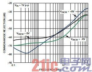
Figure 2. Relationship between CMR and frequency response at different input common-mode voltages
Common mode errors, whether DC offset or AC signals, can degrade video image quality. Figures 3 and 4 show a single large black stripe on a white background. Figure 3 shows the effect of a 500 kHz, 1 V pp common mode noise signal on video image quality. Figure 4 shows the enhanced video image quality with the addition of the ADA4830-1 input stage to remove common mode noise.
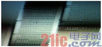
Figure 3. Black streaks of the video after adding 1 V pp, 500 kHz common mode noise, bypassing the ADA4830-1

Figure 4. Black streaks of the video after the ADA4830-1 rejects 1 V pp, 500 kHz common mode noise.
The ADV7180 automatically detects standard analog baseband TV signals compatible with the global NSTC, PAL, and SECAM standards and converts them to 4:2:2 component video data compatible with the 8-bit ITU-R.656 interface standard. For consumer electronics applications with true 8-bit data resolution, accurate 10-bit analog-to-digital conversion provides professional-quality video performance. The three analog video input channels accept standard composite video signals, S-video signals, or component video signals to support a wide range of consumer video sources. Automatic gain control (AGC) and clamp reset circuitry allow the input video signal to peak to peak range of 1.0 V.
Printed circuit board (PCB) layout considerations
In any circuit that emphasizes accuracy, careful consideration must be given to the power and ground return layout on the board. The PCB should isolate the digital and analog sections as much as possible. The PCB is formed by stacking 4 layers of boards with a large area of ​​ground plane and power plane polygon. For a detailed discussion of layout and grounding, see the MT-031 guide; for information on decoupling techniques, see the MT-101 guide.
The ADV7180's power supply is decoupled with 10 μF and 0.1 μF capacitors. In addition, the ADA4830-1 is decoupled with 0.1 μF and 22 μF capacitors to properly reject noise and reduce ripple. These capacitors should be placed as close as possible to the appropriate device to ensure that the 0.1 μF capacitor has a low ESR value. Ceramic capacitors are recommended for all high frequency decoupling.
Make sure the power traces are as wide as possible to provide a low impedance path and reduce the glitch on the power line. The clock and other fast switching digital signals are digitally shielded so that they do not affect other devices on the board.
Common changes
If multiple channels are required, the ADA4830-1 is available in a 2-channel version, the ADA4830-2.
Circuit evaluation and testing
This circuit uses the EVAL-CN0263-EB1Z board, which contains the circuit to be evaluated, as described in this note. The board also includes an ADV7391 video encoder that can be used to reconstruct the input video signal. For an introduction to the output circuit, please refer to the CN-0264 circuit note. The Cypress USB microcontroller is used to configure the EVAL-CN0263-EB1Z board and load software to/from the board.
Equipment requirements
The following equipment is required:
• Windows® XP with a USB port, Windows Vista® (32-bit) or Windows® 7 (32-bit) PC.
• Astrodesign VG-828 programmable video signal generator.
• Used as a video source for single channel and common mode error voltages. The test in this circuit note uses the AD8137 differential amplifier, which converts single-ended video from VG-828 to differential video and applies a 500kHz, 1 V pp common-mode signal to the VOCM input of the AD8137. The output differential signal with the common mode voltage applied is applied to the input of the evaluation board.
• Hewlett-Packard 3314A function generator.
• Agilent E3631A power supply.
• EVAL-CN0263-EB1Z board.
• CN-0263 evaluation software.
• Power: 7.5 V or 7.5 V wall power adapter.
• Video display for viewing the analog video output of the EVAL-CN0263-EB1Z board.
start using
Put the CN-0263 evaluation software CD into your PC and load the evaluation software. Open my computer, find the drive containing the evaluation software CD, and open the Readme file. Follow the instructions in the Readme file to install and use the evaluation software.
Functional block diagram
Refer to Figure 1 of this circuit diagram for the circuit block diagram and the EVAL-CN0263-EB1Z-SCH.pdf file for the circuit diagram. This file is located in the CN0263 Design Support Package.
Setting
In the event of a power outage, connect a 7.5 V supply to the +7.5 V and GND pins on the board. If you have a 7.5 V wall power adapter, you can connect it to the on-board tubular connector instead of the 7.5 V power supply. Connect the Usb Cable to the USB port on your PC. Do not connect the USB cable to the micro USB connector on the board at this time.
test
Power up the 7.5 V power supply (or wall power adapter) connected to the EVAL-CN0263-EB1Z board. Start the evaluation software and connect the PC to the micro USB connector on the PCB via a USB cable.
For more information on how to use the evaluation software to capture data, please refer to the Readme file of the CN-0263 evaluation software.
Radio Alarm Clock,Wake Up Light Alarm Clock,Radio Controlled Wall Clock,Light Alarm Clock
Dongguan Fangbei Electronic Co.,Ltd , https://www.connectorfb.com