On October 26, according to the overall arrangement of the National Twelfth Five-Year Plan 863, the website of the Ministry of Science and Technology released the “Guide to the Application of Major Projects for Efficient Semiconductor Lighting Key Materials Technology R&D†in the New Materials Technology Development Program of the National High Technology Research and Development Program (863 Program). . According to the guide, research and development of energy-efficient, long-life semiconductor lighting products is an important part of the priority theme of the National Medium- and Long-Term Science and Technology Development Plan (2006-2020).
"Energy saving and environmental protection" is the future of mankind, the core of the "Twelfth Five-Year Plan". As a model of low energy consumption and low emissions, the semiconductor lighting industry has become a strategic emerging industry in the national energy conservation and emission reduction targets. As a national strategic technology for the development of next-generation lighting, LED lighting is expected to be the biggest winner in green lighting products.
While the LED lighting industry is developing rapidly, there are also many problems: lack of independent research and development capabilities, lack of industry standards, serious product homogeneity, blind investment, patents and intellectual property rights. Among the many factors affecting its development, the technical problem is currently the primary obstacle facing the domestic LED companies. However, there are few enterprises in China that have mastered LED core technology. Most of them are in the middle and lower reaches of the industry chain; there are only a few domestic enterprises in the upstream industry chain, and production is extremely difficult. The slow progress of the industry's technology, low level of product innovation, and insufficient technical content have led to a lack of core competitiveness in the LED industry.
Throughout the foreign lighting market, European lighting giants Philips and Osram have spent huge amounts of research on the basic technology of LED lighting before 2000. Among them, OSRAM has always been a leader in fluorescent materials for white LEDs.
American CREE, lumileds, bridgeLux and other lighting companies have firmly mastered the core technology of LED chips.
Japan is a world leader in the production technology of high-brightness LEDs and high-grade phosphor technology used in packaging, and Japan has imposed a technical blockade policy. In South Korea and Taiwan, with more mature semiconductor manufacturing and R&D technologies, 70% of the world's high-end LED chip manufacturing is currently completed in this region.
Experiences at home and abroad have proven that LED companies gather through industrial parks and work together to tackle core technologies is an important way to achieve development.
According to the development status of semiconductor lighting technology in China, the core common technology of semiconductor lighting and midstream industry development, cutting-edge technology and key technologies of industrialization have been specifically deployed. The project focuses on improving the international core competitiveness and independent innovation capability of China's semiconductor lighting industry, which is of great significance for realizing China's lighting energy conservation, adjusting the traditional lighting industry structure and cultivating strategic emerging industries.
According to Xu Jian, chief expert of the Expert Group of New Materials in the National 863 Program, according to the “Twelfth Five-Year Planâ€, the localization rate of semiconductor lighting projects will reach 70% by 2015, and the industrial scale will reach 500 billion yuan. The relevant enterprises are facing huge business opportunities. .
The issuance of this document indicates that the government's development plan for the semiconductor lighting industry has evolved from pilot promotion to policy and funding support, which will lead the LED industry to a more professional and orderly direction. Domestic LED lighting companies should also take this opportunity to make clear and specific corporate development plans, and take advantage of technological innovation to concentrate on LED basic technology and core technology research, create a superior innovation environment, and introduce technological innovation talents. Improve the ability of independent innovation and lay the foundation for the future development of enterprises.
Only by mastering advanced technology can we get rid of the restrictions on patents and intellectual property rights of foreign companies, and reduce the production cost of LED products. Only by mastering the technology can we improve the quality of products and get recognition from the market and consumers.
It is also known that Guangdong, as a national LED production province, has cooperated with the Institute of Semiconductors of the Chinese Academy of Sciences, the Guangdong Institute of Industrial Technology, the National Semiconductor Lighting Engineering R&D and Industry Alliance to better integrate the power of science and technology. Established the Guangdong Semiconductor Lighting Industry Technology Research Institute to promote LED technology research.
In the era of knowledge economy, the supporting role of scientific and technological progress and technological innovation in economic and social development will become increasingly prominent. The "Twelfth Five-Year Plan" will be a crucial period for "Made in China" to achieve industrial transformation and leapfrogging. Chinese enterprises need to plan ahead. It is believed that under the guidance of the “Twelfth Five-Year Planâ€, Chinese enterprises will realize “through independent innovation, break through the key technologies of Baiguang general lighting core technology and industrialization, improve the technology innovation system, foster leading talents in science and technology innovation and innovation teams, and establish characteristics. The industrial base will form the strategic goal of the 12th Five-Year Plan for the strategic emerging industries of semiconductor lighting with international competitiveness.

Copper-based PCB, it's the PCB that use copper as the base material and very commonly used in LED products and other electronics products since copper is the material have high heat dissipation.
PCB = printed circuit board and PCBA = printed circuit board assembly. For PCB, it means the copper circuits be printed on a board, and so the main composition of PCB are copper and board.
The copper is the circuits material and the circuits designed by the PCB designers. Depends on the current in the circuits, the PCB copper thickness could be done with 0.5oz-10oz. But the PCB designers need be noted that the copper track width/space need be enlarged with the thickness. For example, the minimum copper track width/space could be 3mil/3mil with 0.5oz, but would be 4mil/4mil with 1oz.
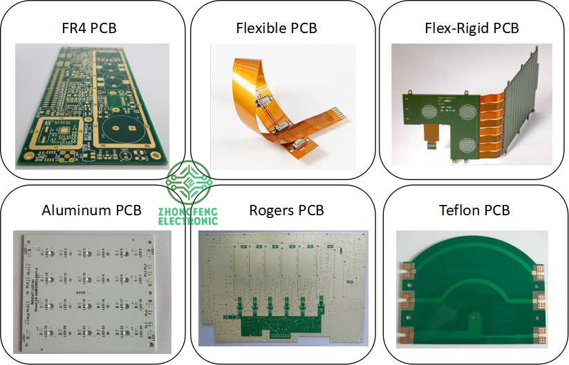
The PCB board could be rigid PCB, could be flex PCB and also could be Flex-Rigid PCB. And the materials could be FR4, PI, Aluminum, Copper-based, Rogers, Teflon, etc. They have different applications. For example, FR4 PCB is the most commonly used for rigid PCB and almost good for all electronics products; PI is the most commonly used for flex PCB; Aluminum and copper-based have good thermal diffusivity and always used for LED PCB ; Rogers PCB and Teflon PCB are always used for High Frequency PCB, etc.
We are the one-stop shop for all kinds of PCB manufacture service from PCB Prototype to big volume, which could save our customers a lot of time and money.
PCB Manufacture Capabilities
|
Features |
Capabilities |
|
Layers |
1-36 layers |
|
Material |
FR-4, Aluminum, Copper, Polyimide, high frequency (Rogers, PTEE, PI), etc. |
|
PCB Type |
FR-4 Standard PCB , Aluminum PCB , Copper-based PCB, HDI PCB , Rigid-Flex PCB, Flex PCB, Thick Copper PCB and Rogers PCB, etc. |
|
Board Thickness |
0.1mm-6.0mm |
|
Copper Thickness |
1/2oz-6oz(18um-210um) |
|
Biggest Board size |
600mm*1200mm |
|
Min Tracing/Spacing |
0.075mm/0.075mm (3mil/3mil) |
|
Min drilling Hole diameter |
0.15mm(6mil), 0.1mm(4mil)-laser drill |
|
Solder Mask |
Green, Black, White, Red, Yellow, Blue and Purple, etc. |
|
Silkscreen color |
White, Blue, Black, Red, Yellow |
|
Surface finish |
HASL Lead free, Immersion Gold (ENIG), Immersion Tin, Immersion Silver, OSP, Carbon oil, etc. |
|
Special Techniques |
Impedance Control, Gold Fingers, Blind/Buried vias, Peelable solder mask, Half holes, Via-in-Pad and Countersink hole, etc. |
PCB Products Show

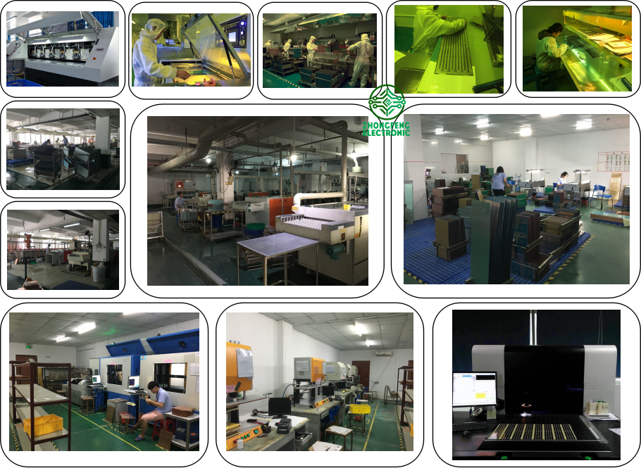
PCB Factory Show

Copper-based PCB
Copper-based PCB,Heavy Copper PCB,Copper Core PCB,Extreme Copper PCB
ZhongFeng Electronic Technology Co., Limited , http://www.dopcba.com
