Abstract: A 1.1W single-channel adaptive filtering Class D audio power amplifier is designed. The power amplifier adopts bilateral symmetric triangular wave as the carrier PWM modulation mode, which effectively reduces the total harmonic distortion of the power amplifier. Test results show that driving a 4Ω load at a 5V supply voltage provides 1.1W of rated output power with an efficiency of up to 90%. The circuit uses a common-mode feedback full-differential amplification input design with high noise rejection ratio, low quiescent current and strong resistance to power supply EMI.
This article refers to the address: http://
introduction
With the continuous development of portable electronic products, the performance of power amplifiers has an important sound for the quality of the products. Traditional linear power amplifiers (A, B, and AB) have good linearity and THD performance, but all have common defects, the efficiency is less than 50%, and the power consumption is large, which restricts the application in portable products. High-efficiency, energy-saving, low-distortion, small-sized D-class amplifiers are increasingly favored by people.
This paper designs an adaptive filtering fully differential audio amplifier with a wide voltage operating range of 2.5V-5.5V, 2.8mA quiescent current, 0.5uA shutdown current, and 250kHz switching frequency inside the chip. The fully differential amplification input of the feedback, the delay start time of 9mS, can effectively prevent the popping interference caused by the starting surge current. The circuit adopts an adaptive filtering structure with high efficiency, low quiescent current and strong resistance to power supply EMI.
1 system circuit design
This paper proposes a chip system as shown in Figure 1. The amplifier is internally composed of a two-stage fully differential amplifier circuit, a PWM waveform comparator, a debounce logic circuit, a logic gate drive output, a delay start circuit, a triangular wave generation circuit, a reference, and an offset. The circuit and the overload protection circuit are composed.
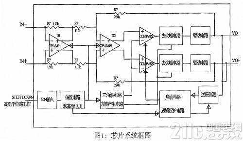
The input differential signal is amplified by a fully differential amplifier and compared to a 250 kHz triangular wave signal to produce a PWM wave. After the waveform is generated, a relatively pure PWM waveform is obtained by shaping the waveform and de-spike the circuit. Then enter the H-bridge drive circuit to output the pulse signal VO+, VO+ to drive the speaker to sound.
2 main unit circuit design and implementation
2.1 Input amplification stage
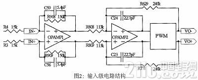
The input amplification signal of the class D power amplifier is realized by a closed loop operation structure. Here two-stage fully differential op amp is used. Figure 2 shows the internal structure of the fully differential op amp. The first stage uses a folded cascode op amp, the second stage uses a common source output stage, and adds Miller compensation to improve the system. Phase margin. As shown in Figure 3.
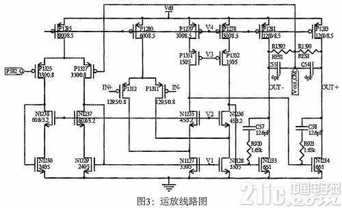
In high-gain fully differential amplifiers, the mismatch of the differential MOS transistors in the input stage and the active load can make the common-mode output level of the fully differential op amp unstable. Therefore, in order to achieve a fixed value of the output common mode level of the fully differential op amp, a common mode feedback network is added to the design. The input signal potential P582_G of the OPAMP op amp in FIG. 3 is equal to the midpoint potential of the triangular wave signal Q2_B. This operation forms a negative feedback in the entire circuit, and the potential of the inverting terminal potential Vout CM signal of the operational amplifier is equal to the potential P582_G of the non-inverting terminal. Thus, the fully differential common mode output potential is stabilized to the potential P582_G.
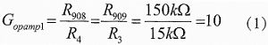
In the first-level fully differential op amp OPAMP1, R3 and R4 are external components, and the internal feedback resistors R908 and R909 are both 150kΩ. The gain of the first stage fully differential op amp is:
In the second-stage fully differential op amp OPAMP2, R808 and R809 have a resistance of approximately 113kΩ and are internal input resistors. R629 and R771 have a resistance of approximately 240kΩ and are internal feedback resistors. The gain of the second stage fully differential op amp is:
![]()
The gain of the entire circuit is 20.
If the external resistance changes then the gain of the entire circuit is:
![]()
2.2 Triangle wave oscillation circuit
The triangular wave oscillation circuit used in this paper is shown in Figure 4. It mainly includes the oscillation core circuit, comparator and latch. The input R182_MINUS signal provides a voltage close to 1/2 Vdd, which is followed by an op amp and applied to R197 to generate a current that is mirrored by the mirrored current source to the R176 and R179 branches, and to the P1634 and N1637 branches. When the triangular wave oscillation circuit operates, the potential of Vc on the capacitor C44 is compared with the potentials of V1 and V2, and the output controls the opening of P1634, N1637, P1635, and N1636.
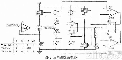
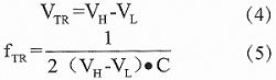
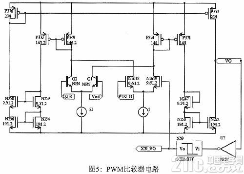
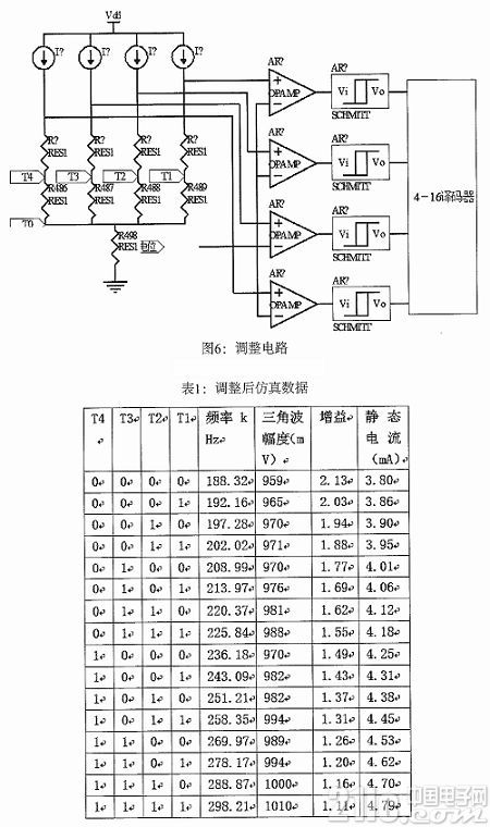
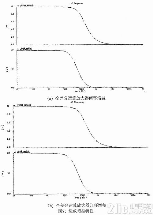
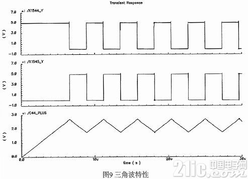
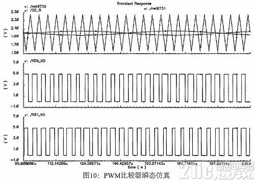
When Vc When V1 When V1 When V1 In the above process cycle, since the current for charging the capacitor C44 is constant, the voltage C44 PLUS on the capacitor is a triangular wave. The signal amplitude VTR and the frequency fTR of the triangular wave generated in Fig. 4 are respectively: A triangular wave having an oscillation frequency of approximately 250 kHz can be obtained. 2.3 PWM comparator circuit The performance of the PWM comparator circuit directly affects the accuracy of the output modulated signal, so high performance comparators with fast time, high slew rate and noise disturbances are needed. The PWM comparator circuit is shown in Figure 5. The Vout signal is the output of the fully differential op amp OPAMP2, and the Q2_B signal is a triangular wave signal. Both signals enter Q1 and Q2 as comparators at the input. The PWM square wave signal X59_VO is output after being shaped by the inverter and the Schmitt trigger X59. This signal X59_VO is fed back to the input of the N2619 of the comparator, and the other N2618 input of the comparator is the midpoint potential P582_G of the triangular wave. When the Vout signal potential is greater than the Q2_B potential, the comparator output terminal VO is low, and the high potential signal X59_VO is obtained after the inverter and the flip-flop. When the signal X59_VO is compared with the potential P582_G, it is more advantageous to make the VO potential low. From the current point of view, when Vout is greater than Q2_B, 8 times of I current flows through the branches of Q1 and P374, and X59_VO is greater than P582_G, so that twice the I current flows through N2619 and P374, so that the total flows through P374. 9 times the current I current. When the Vout signal level is exactly equal to Q2_B, the current flowing through Q2 and the current flowing through Q1 are 4 times I current, then the current flowing through P374 is 5 times I current, and the current flowing through P369 is 4 times current. In this case, the VO will also remain at the original low potential. The entire comparator is like a Schmitt trigger, which has a stabilizing effect on the signal. 2.4 internal frequency and second stage differential gain adjustment circuit The circuit is internally designed to synchronize the gain of the second-stage fully differential op amp and the triangular wave frequency, as shown in Figure 6. In the circuit, the method of selecting and burning four polycrystalline resistors is used to adjust, and the output potential of the 4-wire-16-line decoder is used to control the on and off of the MOS tube to control the internal resistance of the circuit. There are four programming points T1, T2, T3, and T4 in the circuit, plus a common programming point T0. After the resistance was blown, the potential of the branch was high; no burn was low, and the results are shown in Table 1. 3 Simulation results and analysis The cadre spectre simulator was used to simulate the entire circuit using the CSMC0.5UM 5V hybrid process model parameters. The characteristics of the open-loop gain, closed-loop gain, phase margin, and power consumption of the input stage op amp are first simulated. The result is shown in Figure 8, where the power supply voltage Vin=4.6V, Temp=27°C, the low-frequency open-loop gain of the op amp is 110dB, the closed-loop gain is 20 dB, the phase margin is greater than 65deg, and the unity gain bandwidth is 19MHz. It is about 12mW. (a) Fully differential op amp closed-loop gain (b) Fully differential op amp open loop gain The simulation result of the triangular wave oscillation circuit is shown in Fig. 9. X1544 Y corresponds to the Q terminal signal, and X1545 Y corresponds to the QN terminal signal. C44 PLUS corresponds to triangular wave oscillation wave, VH=2.8V, VL=1.5V, and the period of simulation of triangular wave and square wave is 4us. The oscillation frequency is approximately 250 kHz. The output waveform of the comparator circuit is shown in Figure 10. The 5V supply voltage is connected to a 1kHz sinusoidal signal, and the modulated signal is a 250kHz triangular wave signal. It can be seen that when the audio signal changes, the PWM signal flips quickly, avoiding the crossover distortion of the output signal. 4 Summary In this paper, a 1.1W adaptive filtering class D audio power amplifier is designed based on CSMC 0.5UM 5V hybrid process. The input stage op amp circuit and pulse width modulation PWM module and the reference circuit module for generating high precision voltage are mainly introduced. The simulation results show that the designed power amplifier achieves the design requirements of high-performance Class D audio power amplifier under high power conditions. The chip is packaged in BGA form and requires only three components on the periphery. It can be miniaturized in applications and used in PDAs and mobile phones. Split Type Solar Street Lights Split Type Solar Street Lights,Solar Street Light With Pole,Solar Street Light With Camera,Waterproof Solar Street Lighting Jiangsu Bosiwei Optoelectronics Group Co.,ltd , https://www.bswledled.com