
1. Overall design of hardware design
This article refers to the address: http://
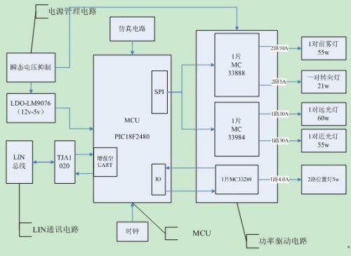
The overall block diagram of the circuit is as follows:
2. Hardware key component selection basis
MCU-PIC18F2480
Its rich on-chip resources are: 16K bytes of on-chip Flash program memory, 768-byte on-chip SRAM, 256-byte EEPROM, 8-channel 10-bit AD, 2 comparators, 2 PWM modules, support for SPI and Master I2C, 33 IO pins, on-chip integrated UART, CAN controller, 1 8-bit timer and 3 16-bit timers. The SPI can implement control and status readback of the driver chip, and the UART can be used to implement the LIN interface.
Power Driver Chips - MC33888, MC33984, MC33289
The MC33984, MC33289, and MC33888 provide control and diagnostics for the SPI. Internal registers are provided for SPI control and diagnostics, and both open-load detection, over-current over-temperature and over-voltage protection are provided.
LIN physical layer transceiver chip-TJA1020
The baud rate is up to 20Kbps, high electromagnetic interference immunity, and extremely low electromagnetic emission emi, providing a sleep mode to meet the requirements of the car for low power consumption.
3. Main hardware modules are divided and interconnected
The hardware circuit includes four main modules: power management circuit, LIN communication circuit, power drive circuit and MCU main circuit. The power management circuit provides working power supply 5v to provide transient suppression and smooth voltage waveform. LIN communication circuit realizes LIN communication and power drive circuit. To achieve drive and fault monitoring of the lamp load, the MCU main circuit provides the main control circuit.
4. Basic hardware principle
a) Power management circuit:
The power management section for the 12V vehicle system, including transient suppression and power supply, provides a stable and abundant power supply to each circuit in the module, taking into account both voltage and current parameters. This module requires three different voltages, the logic voltage is 5V, and the current consumption is usually about 50mA; the LIN transceiver voltage is 5-27V, the typical value is 12V, and the current consumption is 3.5mA; the driving voltage of the lamp is 6V-27V. The typical value is 12V, and the current consumption is relatively large, depending on the lighted lamp load.
For the automotive electrical test standard (B217110) resistance to extreme voltage test requirements, for a 12V network, it is required to withstand a maximum voltage of 24V in 1 minute, and a reverse voltage of 13.5V in 1 minute. There are also test requirements for various transient pulses, mainly for load dumps. Load dump is the situation when the generator is charging the battery and the battery cable is disconnected. At this time, the generator may generate a transient voltage spike of up to 80V. The transient suppression diode SMBJ26CA is used to suppress the transient pulse, which not only suppresses the load. A sudden drop transient, and can also meet the requirement of a maximum voltage of 24V in 1 minute.
Transient (transient) voltage suppression diodes are referred to as TVS devices. Under the specified reverse application conditions, when subjected to a high-energy transient overvoltage pulse, the operating impedance can be immediately reduced to a very low conduction value. Allows large currents to pass through and clamps the voltage to a predetermined level, effectively protecting delicate components in the electronics from damage. The TVS can withstand transient pulse power up to kilowatts and has a clamp response time of only 1 ps. The forward surge current allowed by TVS can reach 50~200A under TA=250C and T=10ms.
The selected transient suppression diode SMBJ26CA can clamp the transient voltage to about 24V, meeting the automotive electronic test requirements.
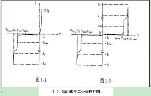
Figure 2: Transient Suppression Diode Characteristics
For voltage reverse protection, because the selected power driver chip MC33888 can withstand a reverse voltage of up to -16V, the driving voltage of the lamp can be directly powered by the voltage after transient suppression. The LIN transceiver voltage can be connected through a diode in series. Reverse protection of the battery voltage is achieved.
For logic circuit 5V, select National Semiconductor's low-dropout (LDO) regulator LM9076BMA, which is an important power device for automotive electronic systems. It has simple application, low external components, low noise, low cost and long-term reliability. Stability and other advantages. National Semiconductor has pioneered an integrated LDO regulator chip that uses a PNP bipolar power stage in its output instead of the traditional bipolar NPN output power stage. The advantage of this change is that the LDO regulator can still provide efficiency for 5V circuits when the voltage drop voltage drops significantly below 1V in the "Cold Crank Condit-ion". LM9076BMA ultra-low quiescent current, 100uA load is only 25uA, output voltage is 5V, accuracy is +/-2% at full temperature and load, 150mA voltage drop is only 200mV, with various protection features such as thermal shutdown, input instant Variable protection and wide operating temperature, input operating voltage up to 40V, withstand transient voltage 70V/-50V, SO8 small package, reduced board size, suitable for demanding automotive electronics applications.
b) LIN communication circuit
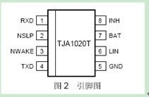
The LIN communication circuit is used to realize the communication between the lamp node and the main node of the LIN network, that is, the combination switch node, and the LIN interface circuit is designed by using the LIN physical layer transceiver TJA1020 and the CPU on-chip peripheral UART. The TJA1020 pins are as shown:
The TJA1020 has three normal modes: normal slope mode, low slope mode, and sleep mode. The preparation mode is the intermediate state. After the TJA1020 is powered on, it first enters the sleep mode, and after being woken up, it enters the preparation mode. The state transition is as shown:
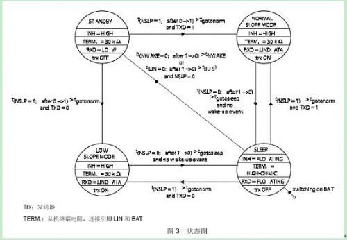
Programming state transitions through statecharts,
Enter sleep mode:
1. Power on automatically enters sleep mode
2. Enter sleep mode from normal slope or low slope mode
3. From the preparation mode, you cannot enter the sleep mode directly. You need to enter the sleep mode via the normal slope or low slope mode.
Enter normal slope / low slope mode:
1. From the ready mode to the normal slope / low slope mode
2. Directly enter the normal slope/low slope mode from sleep mode
3. Normal slope mode and low slope mode cannot be directly converted
Enter the preparation mode:
1. Can only wake up from sleep mode into preparation mode
There are three ways to wake up the TJA1020:
1.LIN remote wakeup
2.NWAKE local wakeup
3. NSLP direct activation
The local wake-up is the NWAKE pin. A low level for a period of time after the falling edge can cause a local wake-up; the remote wake-up is the LIN pin, which is issued by forcing the bus into a dominant bit of 250us to 5ms.
RXD is active low after wake-up and can be woken up by an external INT0 pin interrupt connected to the CPU. The wake-up source can then be determined by the TXD pin. If the TXD is low, it is local wakeup, while the high is remote wakeup. These are all judged in the preparation mode. In the preparation mode, the RXD and TXD of the TJA1020 are used as the IO pins, allowing the MCU to judge the wake-up flag and the wake-up source. After waking up, the CPU will set NSLP high. After setting high, RXD and TXD will be reset immediately, that is, return to high state. The RXD and TXD of the TJA1020 are set to the UART function in normal slope and low slope mode.
The level of the signal in each mode is as shown below:
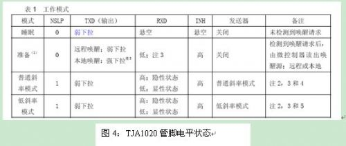
Figure 4: TJA1020 pin level status
c) power drive circuit
The power drive circuit enables control and monitoring of the lamp load in the form of a conventional light bulb. Select Freescale's high-end power switch implementation to provide higher operating frequencies while providing control, protection and diagnostics. The high-end switch chip is selected as shown below. The current parameters are the maximum continuous current.
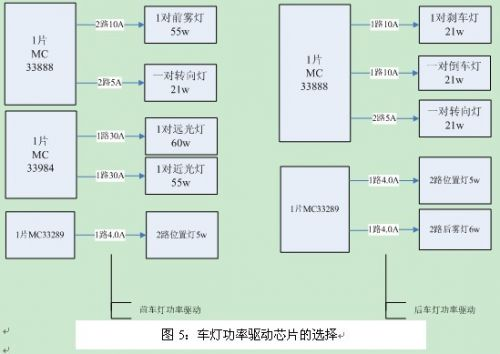
Figure 5: Selection of lamp power driver chip
In the power driver chips of Freescale and Infineon, high-end switch chips and low-end switch chips are available. The high-end channel in the high-end switch chip is used to drive the ordinary light bulb, and the low-end channel in the low-end switch chip is used to drive the LED light. The ordinary bulb and the LED lamp are two different loads. The common bulb is grounded at one end and connected to the high-end switch channel at one end. The LED lamp is connected to the car battery at one end and the low-end switch channel at one end.
The MC33888 has four high-end channels and eight low-end channels. The figure below shows a typical application of a high-side switch channel to drive a normal bulb and a low-side switch channel to drive an LED.
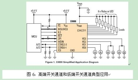
Figure 6: Typical applications for high-side switching channels and low-side switching channels
Both the MC33984 and MC33888 provide control and diagnostics for the SPI. Internal registers are provided for SPI control and diagnostics. The phase and clock polarity of the SPI of the MCU need to be set to match the SPI timing requirements of the MC33984 and MC33888. The MC33289 performs control and status feedback in IO mode. A built-in function to handle the inrush current associated with incandescent lamps is built into the device. The 5A channel in the MC33888 can withstand a peak current of 23A, and the 10A channel can withstand a peak current of 40A.
High-end switching power devices provide load open-circuit detection, over-current over-temperature and over-voltage protection.
The high-end channel is automatically turned off under overvoltage conditions and automatically turns on when it returns to normal. At the same time, the under voltage automatic shutdown protection is provided. When the driving voltage is lower than 6V, the output is automatically turned off. If the driving voltage is not lower than 5V during this period, when the driving voltage returns to above 6V, the output state returns to the state before the automatic shutdown output. If the battery voltage is lower than 5V, the circuit that saves the output state will also be turned off, so that when the battery voltage returns to above 6V, the output returns to the default initialization state.
Not only the corresponding protection measures are provided, but also the function of error detection is provided. The four error states of load open circuit, over voltage, over temperature and over current are represented in real time through a status bit IO port (overcurrent is only for the low end channel). The occurrence of this status bit can be judged by reading the status bit to determine whether an error has occurred. Then the MC33984 and MC33888 can judge the channel with the error status through the SPI. The MC33289 provides one bit for each channel to reflect the status of its channel.
Both Freescale and Infineon's vehicle control solutions leave a margin of 1.5-3 times the drive power, and the margin is designed to improve the long-term stability of a system. The main considerations for the design of the headlight power headroom are the maximum continuous current and cost. When operating at the maximum continuous current, the reliability of long-term continuous operation and the life of the chip cannot be guaranteed, and the problem of heat dissipation must be considered. There is a trade-off between power headroom and cost. The power driver chip selected in Figure 1 is the result of repeated comparisons.
The cost of the front lamp power driver chip is $12, and the cost of the rear lamp power driver chip is $7.2 (official website price).
d) MCU main circuit
As the main controller of this node, the MCU implements the LIN protocol controller, receives the data packet sent by the master node (here, the combination switch node) through the LIN bus, parses the instruction, controls the power drive device, and detects the error. The status information is sent to the master node via the LIN bus to provide diagnostic information.
MCU selects PIC18F2480, its on-chip resources are: 16K bytes of on-chip Flash program memory, 768-byte on-chip SRAM, 256-byte EEPROM, 8-channel 10-bit AD, 2 comparators, 2 PWM modules, SPI support And Master I2C, 33 IO pins, on-chip integrated UART, CAN controller, 1 8-bit timer and 3 16-bit timers. The SPI can implement control and status readback of the driver chip, and the UART can be used to implement the LIN interface.
The peripheral circuit of the PIC microcontroller includes a clock circuit, a reset circuit, and a simulation circuit. The clock circuit selects an external 10M crystal oscillator, and the simulation circuit is used to support the online simulation and programming download of the PIC.
The Multimedia Wiring Harness apply to Audio,Video,Radio, LVDs,Flat RCA,USB.
Yacenter has experienced QC to check the products in each process, from developing samples to bulk, to make sure the best quality of goods. Timely communication with customers is so important during our cooperation.
If you can't find the exact product you need in the pictures,please don't go away.Just contact me freely or send your sample and drawing to us.We will reply you as soon as possible.
Multimedia Wiring Harness
Electric Fan Wiring Kit,Socket Fan Wiring Harness,Custom Pc Wiring Harness,Multimedia Wiring Harness
Dongguan YAC Electric Co,. LTD. , https://www.yacenter-cn.com