
First, the circuit introduction
This article refers to the address: http://
The human body reaction speed tester introduced here is mainly composed of 4 digital circuit chips and 10 LEDs. It can measure the response time of the human body to the signal and divide the reaction time into 8 segments. The higher the number of segments, the faster the reaction speed, often Conducting reaction test training can gradually increase the response speed of the human body.
The reaction tester consists of a power-on delay, a test signal, a clock pulse, a subtraction count, a start display, and a stop control. The figure below is a block diagram of the control principle.
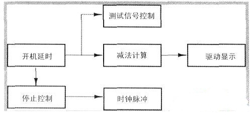
Control principle block diagram
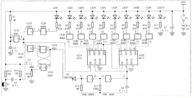
This circuit is mainly composed of three kinds of four CMOS digital integrated circuits. The circuit schematic is shown below. IC1 is a four-input or non-gate circuit 4001. IC3 and IC4 are inverters 4069. Each chip contains six independent inverters, which have a large current driving capability and can directly drive the LEDs. The pin numbers of the integrated circuits are marked in the schematic diagram. For more detailed chip characteristics, refer to the relevant materials.
Among them, IC2 selects the dual 4-bit static shift register 4015. The pin function is shown in the figure on the right (omitted). It contains two independent 4-bit serial-in-one-out shift registers, which are cascaded in this circuit. Each set of registers has a clock terminal CLK, a clear terminal RST, and a serial data input terminal D. The output of each register unit is derived, so both serial output and parallel output can be performed. The data applied to the D terminal is shifted to the right by the rising edge of the clock. When "1" is added to the clear terminal RST, all registers are zero. Two sets of registers are used in cascade in this circuit. The truth table for 4015 is shown in the table below.
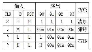
4015 truth table
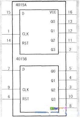
IC2 selects dual 4-bit static shift register 4015
Second, the working process of the circuit
After the power switch K1 is closed, the power indicator LED10 is turned on, and then delayed by a few seconds, the test signal LED1 is lit, the subtraction counter circuit starts to decrement under the action of the clock pulse, and the test consisting of LED2~LED9 shows that the light-emitting tube is extinguished in turn, During the process, when the test subject presses the stop button K2, the clock pulse is stopped, the subtraction counter is in the hold state, and the number of LED2 and LED9 extinguished will be recorded as the reaction time of the test subject.
Third, the working principle of the circuit
The multi-vibrator consists of IC4E, IC4F, R16, R17, C4, etc. As the clock pulse, the oscillation period is about 212×R17×C4. According to the parameter period of Figure 3, the parameter period is about 44rns, and IC2(4015) is composed of 8 bits. The shift register, IC1B, R1, C1, etc. constitute a boot delay circuit. When the power switch K1 is just closed, the output of IC1B is "1". Under the action of the clock pulse, the 8-bit register unit of IC2 is all "1" quickly. After a few seconds, the output of IC1B becomes "0". After the two stages of IC3A and IC3B are reversed, the driving test signal LED1 is lit. At the same time, the 8-bit register unit of IC2 will change to "0" from left to right under the action of the clock pulse. When the tester presses the stop button K2, the RS flip-flop composed of IC1C and IC1D is set to "O". The IC4E and IC4F are stopped, and the IC2 is in the hold state. As a result, the LEDs are driven by IC3C to IC4D. The function of IC1A here is that only when the test signal LED1 is lit, pressing the stop button K2 can be effective. Pressing K2 in advance is invalid.
How the circuit works
Fourth, the production process
A photo of the complete set of components of this tester is shown below (omitted). The list of components is shown in the table below. It is recommended to check the component parameters and quantity one by one according to the component list before assembly. Assembly can begin as soon as possible. The order of the welding elements is in principle followed by a short, high, small and large.
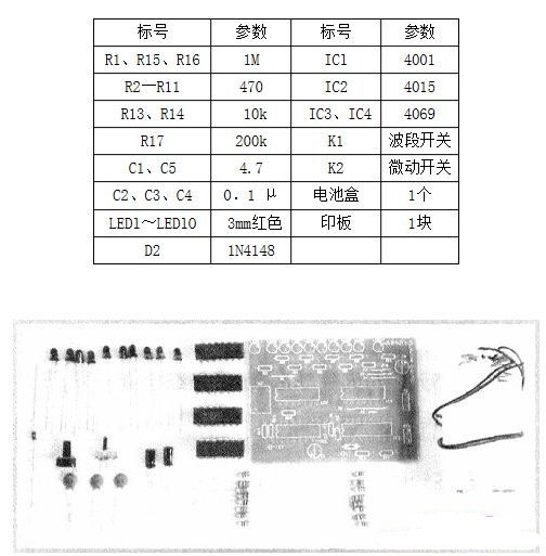
Complete set of testers
The figure below shows the component position installation diagram. The integrated circuit chip is viewed from the front, and the side with the semicircular notch is turned to the left, and the chip is inserted on the printing plate according to the logo on the printing plate. The recommended welding sequence is:
(1) Soldering resistors, jumpers (J1 to J6), and diodes 1N4148.
(2) Soldering ceramic capacitors, electrolytic capacitors, switches, and buttons.
(3) Welding 10 LEDs.
(4) Solder four CMOS integrated circuit chips.
(5) After all is completed, carefully check whether each solder joint is secure, and do not have short circuit or open circuit. If necessary, you can turn the board toward the light and check the welding.
After the determination is correct, the battery leads are soldered. Note that the positive and negative leads are distinguished. Then load 4 No. 5 batteries to test the power.
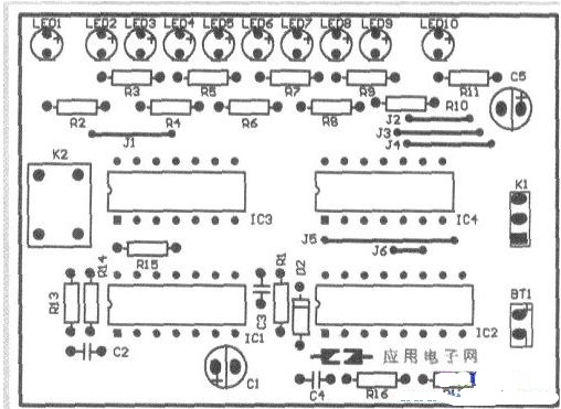
Component position installation diagram
Five, welding precautions
When soldering CMOS digital integrated circuits, pay attention to the soldering iron to be grounded reliably, or unplug the power plug with residual heat to prevent the induced static electricity from penetrating the CMOS chip. There are 6 jumpers on the printed board, which are represented by J1 - J6 respectively, and can be soldered by the excess component pin lines cut. The longer one of the LED pins is the positive pole, and the outer circle with a small straight section is the negative pole, which can be installed according to the character mark on the printed board. One end of the 1N4148 diode body with a black ring is the negative pole. C1 and C5 are electrolytic capacitors. The shorter end of the pin is the negative pole, and the outer skin is usually marked with “—â€. The lead of the battery case is correctly connected according to the "+" and "-" polarity of the printed board mark, and must not be reversed. After all components have been soldered, check carefully to see if the components are properly installed, solder joints are secure, and there is a short circuit between the pads and traces to ensure proper assembly.
Sixth, power-on test
After the comprehensive inspection is completed, the battery can be connected for testing.
When the power switch K1 is closed, the LEDs 10 are lit, indicating that the power is turned on, and then the LEDs 2 to 9 are quickly turned on. After a delay of a few seconds, the LED 1 is lit, indicating that the test is started, and the LEDs 2 to LEE 9 are quickly turned off. At this time, when the stop button K2 is pressed, the LEDs 2 to 9 are immediately stopped and turned off, and the state is retained. Since the period of the multivibrator is about 44 ms, by calculating the number of extinctions of the LEDs 2 to 9 , the reaction speed of the test subject can be calculated. For example, after pressing the stop button, a total of 4 LEDs of the LED 2 LED 5 are extinguished, then The tester's reaction rate was 44 ms x 4 = 176 ms, or 0.176 s. If the circuit is not working properly, please check the assembly correctly. According to the working process, check the fault point step by step according to the schematic diagram.
In fact, by changing the parameters of R17 or C4, the frequency of the multivibrator can be adjusted, and the test speed can be changed, which has increased or decreased the test difficulty. Changing the parameters of R1 and C1 can change the time after the power-on, the test delay starts, so that the testee can not master the test rule and improve the accuracy and interest of the test. When the second test is required, turn off the power switch K1 for a few seconds, then turn it on again to perform a new test.
Garden Lamp is a kind of outdoor lighting lamps and lanterns, usually refers to the outdoor Road Lighting lamps and lanterns below 6 meters.The Garden Lamp is characterized by its diversity, beauty and decoration environment, so it is also called landscape courtyard lamp.Slow lane, narrow lanes and is mainly used in city residential areas, tourism scenic area, outdoor lighting, park, plaza and other public venues can prolong people's outdoor activities, improve the security of the property.

The Garden Lamp has many styles, each style has its own unique name.For example, Water,Moon,Diamonds,Lucky and UFO, these garden lights are not only elegant in name, but also artistic and elegant in appearance.
The Garden Lamp body is aluminium alloy profile is used for manufacturing, high strength, light pole electrostatic powder spraying process, anti graffiti proof, radiation stainless steel links, anti-corrosion ability, patent luminous light pole, the built-in LED light source, disassembling design is reasonable, easy to install and maintain, installation height is 3 to 5 meters.


Technical parameters
|
Chip |
CREE/SAMSUNG/PHLIPS |
|
Initial luminous flux |
≥90LM |
|
Color temperature |
3800-6000K |
|
Level of protection |
IP65 |
|
Power factor |
0.96 |
Garden Lamp
Garden Lamp,Garden Lamp Post,Garden Lamps Solar,Garden Lamp Post Solar
Jiangsu chengxu Electric Group Co., Ltd , https://www.satislighting.com