
How to choose the right components and parameters for the switching power supply circuit?
Many engineers who have not used switching power supply design will have certain fears, such as concerns about switching power supply interference, PCB layout problems, component parameters and type selection issues. In fact, as long as you understand, the use of switching power supply design is very convenient.
A switching power supply generally consists of a switching power supply controller and an output. Some controllers integrate the MOSFET into the chip, which makes it easier to use and simplifies PCB design, but the design flexibility is reduced.
The switch controller is basically a closed-loop feedback control system, so there is generally a sampling circuit that feeds back the output voltage and a control loop for the feedback loop. Therefore, this part of the design is to ensure accurate sampling circuit, and to control the feedback depth, because if the feedback loop response is too slow, it will have a great impact on the transient response capability.
The output part design includes output capacitors, output inductors, MOSFETs, etc. These devices are basically designed to meet the balance of performance and cost. For example, high switching frequency can use small inductance values ​​(meaning small package and cheap) The cost), but the high switching frequency increases the interference and switching losses to the MOSFET, resulting in reduced efficiency. The result of a low switching frequency is the opposite.
The ESR of the output capacitor and the Rds_on parameter selection of the MOSFET are also critical. A small ESR can reduce the output ripple, but the cost of the capacitor will increase, and a good capacitor will be expensive. Switching power supply controller drive capability should also be noted that too many MOSFETs cannot be driven well.
In general, the supplier of the switching power supply controller will provide specific calculation formulas and usage plans for engineers to learn from.
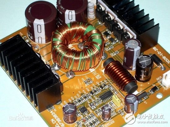
Internal structure of switching power supply
How to debug the switching power supply circuit?
Some experience can be shared with everyone:
(1) The output of the power supply circuit is connected to the board through a low-resistance high-power resistor, so that in the case of no soldering resistor, the power circuit can be debugged first, avoiding the influence of the latter circuit.
(2) Generally speaking, the switch controller is a closed-loop system. If the output deteriorates beyond the range that the closed-loop can control, the switching power supply will not work properly. Therefore, the feedback and sampling circuits need to be carefully checked. In particular, if a large ESR output capacitor is used, a lot of power supply ripple will occur, which will also affect the operation of the switching power supply.
Why should we ground?
The introduction of grounding technology was originally designed to prevent lightning strikes on equipment such as electricity or electronics. The purpose is to introduce the lightning strike current generated by lightning into the earth through a lightning rod to protect the building. At the same time, grounding is also an effective means to protect personal safety. When the phase line caused by some reason (such as poor wire insulation, aging of the line, etc.) and the equipment casing touch, the equipment's outer casing will have dangerous voltage. The generated fault current flows through the PE line to the ground for protection. With the development of electronic communication and other digital fields, it is far from satisfactory to consider only lightning protection and safety in the grounding system. For example, in a communication system, the interconnection of signals between a large number of devices requires that each device have a reference 'ground' as a reference ground for the signal. Moreover, with the complication of electronic devices, the signal frequency is getting higher and higher. Therefore, in the grounding design, electromagnetic compatibility problems such as mutual interference between signals must be given special attention. Otherwise, improper grounding will seriously affect the reliability of the system operation. Sex and stability. Recently, the concept of "ground" has also been introduced in the signal reflow technique of high-speed signals.
Grounding definition
In modern grounding concepts, for line engineers, the term is often referred to as "the reference point for line voltage"; for system designers, it is often a cabinet or rack; for electrical engineers, it is green Safe ground or the meaning of receiving the earth. A more general definition is "ground is the low impedance path where current returns to its source." Note that the requirements are "low impedance" and "path".
Common ground symbol
PE, PGND, FG-protective ground or chassis; BGND or DC-RETURN-DC-48V (+24V) power supply (battery) reflow; GND-work ground; DGND-digital ground; AGND-analog ground; LGND- lightning protection Protected land.
Suitable grounding method
There are several ways to ground, single point grounding, multi-point grounding, and mixed type grounding. Single-point grounding is divided into series single-point grounding and parallel single-point grounding. In general, single-point grounding is used for simple circuits, grounding between different functional modules, and low-frequency (f10MHz) circuits require multi-point grounding or multi-layer boards (complete ground plane layers).
Introduction to signal reflow and cross-segmentation
For an electronic signal, it needs to find a way to return the current with the lowest impedance to the ground, so how to handle this signal reflow becomes very critical.
First, according to the formula, the radiation intensity is proportional to the loop area, that is, the longer the path that the reflow needs to go, the larger the loop formed, and the greater the interference with the external radiation. Therefore, when the PCB is laid Minimize power supply loop and signal loop area.
Second, for a high-speed signal, providing good signal reflow can guarantee its signal quality. This is because the characteristic impedance of the transmission line on the PCB is generally calculated by reference to the ground plane (or power plane), if the high-speed line There is a continuous ground plane nearby, so that the impedance of this line can be kept continuous. If there is no ground reference near the segment line, the impedance will change, and the discontinuous impedance will affect the signal integrity. Therefore, when wiring, you should assign the high-speed line to the layer near the ground plane, or walk along the high-speed line and walk one or two ground lines to provide the function of shielding and providing reflow.
Third, why do you try to avoid splitting across the power supply when wiring? This is because after the signal crosses different power supply layers, its return path will be long and susceptible to interference. Of course, it is not strictly required that it cannot be split across power sources, and it is possible for low-speed signals because the generated interference can be ignored regardless of the signal. For high-speed signals, it is necessary to carefully check, try not to cross, you can adjust the wiring of the power supply part.
Why separate the analog ground from the digital ground and how to separate it?
Both analog and digital signals are returned to ground because the digital signal changes rapidly, causing a large amount of noise on the digital ground, and the analog signal requires a clean ground reference. If the analog ground and digital ground are mixed together, the noise will affect the analog signal.
In general, analog ground and digital ground are treated separately, then connected together by thin traces, or joined together at a single point. The general idea is to try to block the noise on the digital ground from hitting the analog ground. Of course, this is not very strict. The analog ground and the digital ground must be separated. If the digital ground near the analog part is still very clean, it can be put together.
How is the signal on the board grounded?
For general devices, the nearest grounding is the best. After using a multi-layer board design with a complete ground plane, it is very easy to ground the general signal. The basic principle is to ensure the continuity of the trace and reduce the number of vias. Close to the ground plane or power plane, and so on.
How is the interface device of the board grounded?
Some boards have external input and output interfaces, such as serial port connectors, network port RJ45 connectors, etc. If the grounding of them is not well designed, it will affect normal operation. For example, the network port interconnection has errors and is lost. Packages, etc., and will become external sources of electromagnetic interference, sending out the noise inside the board. Generally, a separate interface ground is separately separated, and the connection with the signal ground is connected by a thin trace, and a resistor of 0 ohm or small resistance can be serially connected. Fine traces can be used to block signal ground noise from reaching the interface ground. Similarly, the filtering of the interface ground and interface power supply should also be carefully considered.
Cable with shield, how is the shield grounded?
The shielding layer of the shielded cable must be connected to the interface ground of the board instead of the signal ground. This is because there is various noise on the signal ground. If the shield layer is connected to the signal ground, the noise voltage will drive the common mode current along the shield layer. Interference, so poorly designed cable is generally the largest source of noise for electromagnetic interference. Of course, the premise is that the interface should be very clean.
PVC Rare Earth Aluminum Alloy Power Cable is kind of cable, in which the rare earth high compressed aluminum alloy is used as conductor, and PVC is used as insulation and Jacket. It has completely independent intellectual property rights and removed the defects of aluminum cable systematically. It applies to both dry and moist places at the temperature of 75ºC and under, and the temperature of short circuit is 160ºC. The alloyed material greatly improves the toughness and high creep resistance. Due to its low density compared to copper wire and high strength, Aluminum Alloy Wire is preferred by customers.

Standard: GA306 Jacket: PVC
Conductor: aluminum alloy Cores: single core or multicores
Insulation: PVC Rated voltage: 0.6/1KV
Advantages:
- Conductor fatigue resistance
- Creep resistance
- Impact resistance
- Easy to bend
- Light weight
- Easy installation
- Long life span
- Flame retarded
- Fire resistant
- Zero halogen & low smoke
- Corrosion & abrasion resistant
- Decent mechanical strength
- Chemical & acid resistance
- ...

Application:
- Lighting
- High rising buildings
- Public Buildings
- Family residence
- Household appliances
- Electrical equipment
- Power console
- Automotive industry
- Government buildings
- Power transmission and distribution lines
- And many more...
Welcome to visit our factory to learn more about us. If you have any questions, please feel free to contact us.
PVC Insulated And Sheathed Alloy Cable
PVC Insulated And Sheathed Alloy Cable,PVC Insulated Alloy Cable,PVC Sheathed Alloy Cable,Insulated PVC Jacket Power Cable
Smartell Technology Co.,Ltd , http://www.liencable.com