
introduction
Due to the wide application of MOSFET and IGBT and soft switching technology in power electronic circuits, the switching frequency of power converters is getting higher and higher, and the structure is more compact, but it also brings many problems, such as the influence of parasitic components, electromagnetic radiation. Intensified, etc., so EMI is one of the major concerns of the power electronics industry.

Conduction is an important means of interference propagation in power electronics. Differential mode interference and common mode interference are the main forms of conducted interference. In most cases, the conducted interference of the power converter is dominated by common mode interference. This paper introduces a passive common mode interference suppression technique based on the compensation principle and successfully applied to various power converter topologies. Both theoretical and experimental results demonstrate that it can effectively reduce high frequency conducted common mode interference in the circuit. The advantage of this solution is that it does not require additional control circuits and auxiliary power supplies, and does not depend on the operation of other parts of the power converter. The structure is simple and compact.
1 Compensation principle
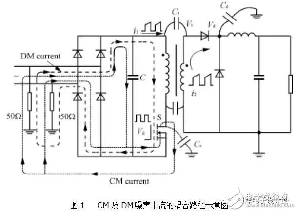
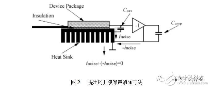
Common mode noise is different from the internal mechanism of differential mode noise: differential mode noise is mainly caused by the ripple current of the switching converter; common mode noise is mainly caused by the interaction between higher d/d and spurious parameters. Caused by high frequency oscillations. As shown in Figure 1. The common mode current contains the displacement current that is wired to the ground plane. At the same time, since the d/d at the terminal of the switching device is the largest, the stray capacitance between the switching device and the heat sink will also generate a common mode current. Figure 2 shows the essential concept behind this new common mode noise suppression circuit. The d/d of the switching device forms a noise current to the ground through a parasitic capacitance between the housing and the heat sink. The suppression circuit detects the d/d of the device and inverts it and then adds it to a compensation capacitor to form a compensation current that cancels the noise current. That is, the compensation current and the noise current are equal in amplitude but 180° out of phase, and also flow into the ground plane. According to Kirchhoff's current law, the two currents sink at zero at the ground point, so the common mode noise voltage on the 50Ω impedance balance network (LISN) resistor (connected to the BNC port of the measurement receiver) is greatly reduced.
Application of Common Mode Interference Suppression Technology Based on Compensation Principle in Switching Power Supply
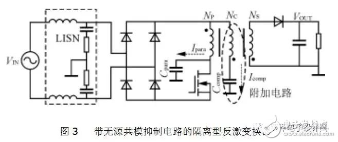
In this paper, the single-ended flyback circuit is taken as an example to introduce the application of common mode interference suppression technology based on compensation principle in power converter. Figure 3 shows the topology of a typical single-ended flyback converter with the addition of a new common-mode noise suppression circuit. As shown in FIG. 3, the parasitic current caused by d/d from the switching device is para injected into the ground layer, and the inverted noise compensation current comp generated by the additional suppression circuit is also injected into the ground layer. The ideal situation is that the two currents are summed to zero, which greatly reduces the common mode current flowing to the LISN resistor. An additional winding NC is added to the original winding structure using the power transformer core in the existing circuit. Since the winding only needs to flow through the reverse noise current generated by the compensation capacitor comp, its wire diameter appears to be small relative to the original and secondary P and S windings (determined by the design considerations of the actual device). The compensation capacitor comp in the additional circuit is mainly used to generate a compensation current that is inverted from the parasitic noise current caused by the parasitic capacitance para. The size of comp is determined by para and winding turns ratio P:C. If P:C=1, the capacitance value of comp is equal to para; if P:C≠1, the value of comp satisfies comp=para·d/d.
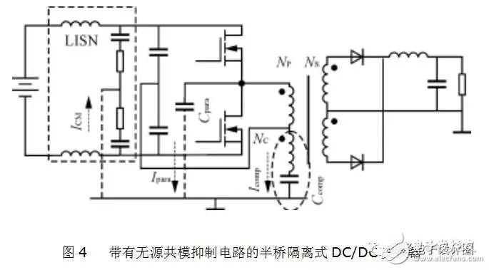
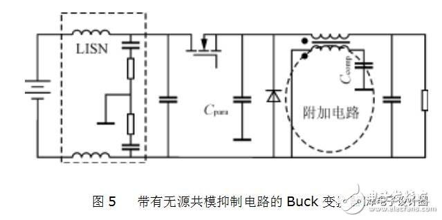
In addition, it is also possible to form a passive compensation circuit by modifying an inductor or a transformer in a DC/DC converter such as Buck, Half-bridge, etc., to achieve noise suppression, as shown in FIG. 4 and FIG.
The experiment used a single-ended flyback auxiliary power supply of a 5kW/50Hz marine inverter as an experimental platform. The output of the AC voltage regulator is fed into the rectifier bridge via the LISN, and the rectified DC output is used as the input to the flyback circuit. The multi-point measured collector electrode has a parasitic capacitance of about 80pF to the experimental ground (chassis). In view of the existing capacitive components in the laboratory, a 100pF, 1kV ceramic capacitor is used as the compensation capacitor. A grounded aluminum plate is used as the experimental desktop, and the outer casing of the LISN and the flyback power supply to be tested are well grounded. Figure 6 is the compensation winding voltage and the original winding voltage waveform. The accurate inversion of the compensation winding reproduces the waveform of the primary winding. Figure 7 is a waveform of the current flowing through the compensation capacitor and the parasitic current of the switch tube heat sink to ground. It can be seen from Fig. 7 that the phase of the compensation current and the parasitic current waveform are 180° out of phase, which is also in good agreement with some waveform spikes. However, since the metal casing of the switch tube is a collector and communicates with the heat sink, the irregular shape of the heat sink causes uncertainty in the measurement of the parasitic capacitance of the switch tube. It can be seen from Fig. 7 that the amplitude of the compensation current is larger than the actual parasitic current, indicating that the value of the compensation capacitor and the parasitic capacitance are not sufficiently good, and the value is slightly larger. Figure 8 shows a comparison of the common mode current waveforms flowing into the LISN ground line before and after the compensation circuit is added. After the current balance of the common mode suppression circuit, the peak of the common mode current is well suppressed. The experimental data shows that the maximum suppression is about 14 mA.
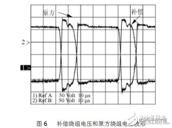
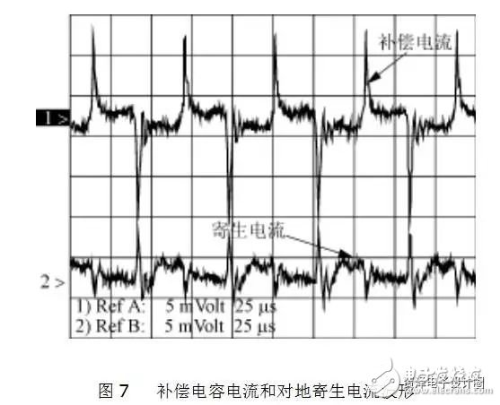
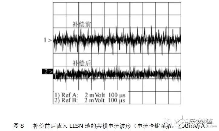
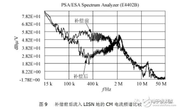
Figure 9 is a spectral waveform of the common mode current measured with an Agilent E4402B spectrum analyzer. It can be seen that the CM noise in the frequency range of 100 kHz to 2 MHz is well suppressed. However, an amplitude protrusion appeared around 3MHz, and there was no obvious attenuation in the high frequency band. This shows that under high frequency conditions, the distribution parameters of the circuit become the main influencing factors of noise coupling, and the compensation circuit brings high The frequency oscillation also partially increases the high frequency component of the common mode EMI noise. However, from a filter design point of view, this does not affect much the equipment cost saved by lowering the low harmonic noise. If the compensation capacitor can be adjusted more accurately as close as possible to the value of the parasitic capacitance Cpara, the suppression effect will be improved on this basis.
4 Limitations of this technology
(a), (b), (c), and (d) in Fig. 10 show waveform simulations of voltage and current when the noise suppression circuit cannot function normally. There are two main situations here:
The first case is encountered on the equivalent series inductance of the input capacitor. The inductor acts as a limiting current rate of change d/d throughout the circuit. It is clear that the series inductance of the large inductance in the LISN limits the ability of the converter supply as a current source. Therefore, the energy required for these ripple currents must be supplied by the input capacitance, but the input capacitance itself also limits their ability to act as a current source. The larger the input capacitor is, the more limited it is to provide the high frequency current required to compensate the transformer. When it is 100nH, the compensation circuit is almost ineffective. Although the compensation voltage is very similar to the parasitic CM voltage waveform in Fig. 10(a), it is apparent in Fig. 10(b) that the current flowing through the compensation capacitor comp is limited.
Another serious situation is to compensate for the leakage inductance of the transformer. When the transformer leakage inductance is increased from 0.1% of the original magnetizing inductance to 10%, the compensation circuit also begins to fail, as shown in Figure 10(c) and Figure 10(d). The compensation winding voltage waveform is bifurcated due to leakage inductance and magnetizing inductance. If the leakage inductance is small relative to the magnetizing inductance, the waveform distortion can be neglected, but the d/d waveform presented on the actual compensation capacitor has deteriorated, so that the compensation circuit cannot effectively suppress.
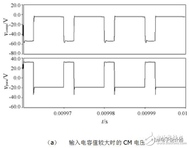
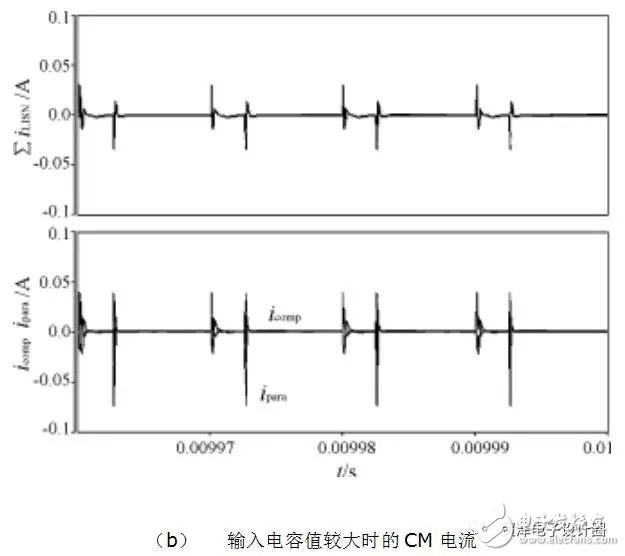
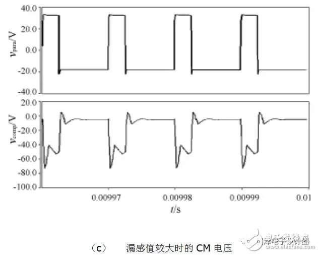
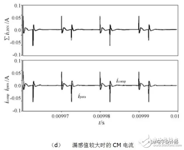
Figure 10: Noise circuit failure simulation voltage and current waveform
In order to solve the two serious limiting factors of transformer leakage inductance, the following measures can be taken: for the input capacitor, it should be reduced to an acceptable level, and improved by paralleling low-value capacitors; close-wound original winding and compensation winding Can effectively reduce the leakage inductance.
5 Conclusion
It can be seen from the above experiments and analysis that such a passive CM noise suppression circuit applied to a conventional power converter topology has a certain effect. Since the additional windings used for compensation only need to be added to the existing transformer structure, the isolated topology may be the simplest and most economical circuit structure for employing such passive compensation cancellation circuits.
Function description
The socket is ordinary converter,with two output 5V2A power USB power supply at the same time,can be very convenient in use electrical appliances and recharge the equipment at the same time,such as digital products like Iphone Ipad,MP3,MP4 etc.The charge apply to full range of international AC output,no-load power consumption less than 0.3W,with short circuit,overload,over-voltage protection,can be convenient for your life and save more energy
Timer Control Time Adgustment
1.Press the power switch 1 time,the 1HOUR LED will light on.The Timer into ON mode,USB and control socket output ON .
2.Continuously press the power switch the LED light on,the Countdown mode and LED light on will cycle change from 1HR,2HR,4HR,6HR,8HR,10HR.
3.Choose you need countdown time mode,the mode LED will lighto on,start countdown until countdown time finish,the control output and USB change to OFF
4.Then the countdown is start,The Time indicate LED will from high to low auto change until Countdown finish off.
Failure analysis:
1.check whether the power supply connection is good
2.check whether the USB cable is loosen
Warning Note:
1.Use indoor and dry location ONLY
2.The load max does not exceed 15A 3600W
3.This product does not convert voltage please do not miss use DO NOT exceed the maximum loading of 3600 Watts 15A
4.Always have earth connection for safety reason
5.If in doubt please consult with a qualified electrician
USB charger socket, USB socket, USB plug, USB plug socket
NINGBO COWELL ELECTRONICS & TECHNOLOGY CO., LTD , https://www.cowellsocket.com