
Basic Principles of DDS Architecture
With the increasing use of digital technology in instrumentation and communication systems, digital control methods that generate multiple frequencies from a reference source have emerged. This is known as Direct Digital Frequency Synthesis (DDS). The basic structure of a DDS system is illustrated in Figure 1. In this simplified model, a stable clock drives a programmable read-only memory (PROM) that contains one or more cycles of a sine wave or another arbitrary waveform. As the address counter progresses through each memory location, the corresponding digital amplitude values are sent to a Digital-to-Analog Converter (DAC), which produces an analog output signal. The spectral purity of the final output is primarily determined by the DAC, while phase noise mainly comes from the reference clock.
Being a sampled data system, DDS must account for several factors like quantization noise, aliasing, and filtering. For instance, higher harmonics of the DAC output frequency can fold back into the Nyquist bandwidth and become unfilterable, unlike in PLL-based synthesizers where such harmonics can be filtered out. Additional considerations will be discussed later.
Figure 1: Basic principle of a direct digital frequency synthesis system
The main limitation of this simple DDS setup is its inflexibility—changing the output frequency requires either adjusting the reference clock or reprogramming the PROM. In real-world applications, a more flexible approach is used: a Numerically Controlled Oscillator (NCO), shown in Figure 2.
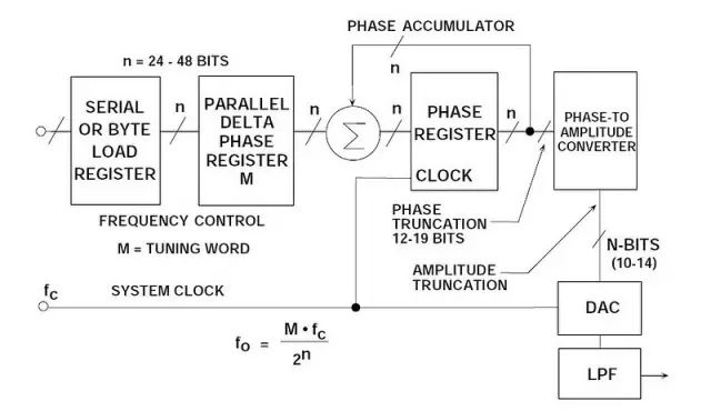
Figure 2: Flexible DDS System
At the core of the system is a phase accumulator, which updates its contents with every clock cycle. Each time it updates, a value M from the delta phase register is added to the current phase value. If M is set to 1, the phase accumulator will take 2^32 clock cycles to complete a full cycle. This mechanism allows precise control over the output frequency.
The truncated output of the phase accumulator serves as the address for a sine (or cosine) lookup table. Each entry in the table corresponds to a specific phase point of the sine wave, typically covering 0° to 360°. Only 90° of data is needed due to symmetry, making the lookup table efficient. This mapping enables the generation of accurate digital amplitude values that drive the DAC.
Figure 3 illustrates how the phase accumulator’s output forms a "phase wheel," representing the continuous progression of phase values. When M increases, the phase accumulator rolls faster, resulting in a higher output frequency. This relationship is described by the DDS tuning formula:
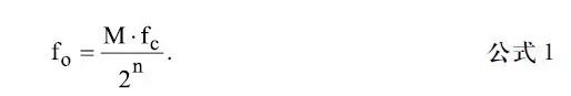
Figure 3: Digital Phase Wheel
This formula shows that the output frequency depends on the clock frequency (fc) and the number of phase increments per cycle (M). The resolution of the system is fc / 2^n, where n is the width of the phase accumulator. With n = 32, the resolution is over 4 billion, allowing for extremely fine frequency control.
In practice, the overflow bits of the phase accumulator are often truncated, leaving only the most significant bits (MSBs) to address the lookup table. This reduces the size of the lookup table without significantly affecting the frequency resolution. Truncation introduces minimal phase noise, which is usually acceptable.
Figure 4 demonstrates the performance of a 15-bit phase accumulator with 15-bit truncation. The calculated output spectrum shows a Spurious-Free Dynamic Range (SFDR) of 90 dB, far exceeding typical commercial 12-bit DACs. Even with some quantization noise, the performance is sufficient for most applications.
Figure 4: The calculated output spectrum shows 90 dB SFDR at 15-bit phase truncation
The DAC's resolution is usually 2–4 bits less than the lookup table's width. A perfect N-bit DAC still introduces quantization noise, but in modern DDS systems, these effects are well managed. The combination of phase truncation and DAC resolution results in spurs that are at least 90 dB below the main signal, ensuring high-quality output.
The flexibility of the basic DDS system allows for immediate frequency changes without phase discontinuities. However, in actual implementations, the new frequency word must be loaded into an internal buffer before being transferred to the phase accumulator. This process ensures minimal pin count and smooth transitions between frequency settings.
Aliasing in DDS Systems
An important limitation in DDS systems is the range of output frequencies. According to the Nyquist criterion, the clock frequency must be at least twice the output frequency. In practice, the maximum output frequency is limited to about one-third of the clock frequency. For example, with a 100 MHz clock, the maximum output frequency is around 30 MHz. Aliasing occurs when higher harmonics of the output frequency fall within the Nyquist band, making them difficult to filter out.
Figure 5 shows a 30 MHz output with a 100 MHz clock. An anti-aliasing filter is necessary to remove the image frequency at 70 MHz. Additionally, the DAC output has a sin(x)/x response, causing a roll-off at higher frequencies. This effect can be compensated using a filter with a transfer function designed to flatten the overall frequency response.
Figure 5: Aliasing in a DDS system
Another challenge is that the harmonics of the fundamental frequency in a DDS system can fold back into the baseband due to aliasing. These harmonics cannot be removed by standard filters, leading to spurious signals in the output. For example, with a 100 MHz clock and a 30 MHz output, the second harmonic appears at 60 MHz (out-of-band) and 40 MHz (aliased), and so on for higher harmonics.
DDS System Used as an ADC Clock Driver
DDS systems like the AD9850 are ideal for generating ADC sample clocks, especially when the sample frequency needs to be software-controlled and synchronized with the system clock. The DAC output drives a low-pass filter that removes spurious components above 42 MHz, ensuring clean signal integrity. The filtered output can then be used to trigger the ADC’s internal comparator.
The comparator produces a square wave with a rise and fall time of 2 ns, compatible with TTL/CMOS logic levels. The jitter at the output edge is less than 20 ps RMS, making it suitable for high-speed applications. Additional outputs and compensation features are available upon request.
Figure 6: Using a DDS System as an ADC Clock Driver
In the circuit shown in Figure 6, the total RMS jitter of the 40 MSPS ADC clock is 50 ps, which may affect the signal-to-noise ratio in wide dynamic range applications.
Amplitude Modulation in DDS Systems
Amplitude modulation in a DDS system can be achieved by placing a digital multiplier between the lookup table and the DAC input, as shown in Figure 7. Alternatively, the DAC’s reference voltage can be adjusted to modulate the output amplitude. In the AD9850, the internal reference amplifier has a bandwidth of about 1 MHz, making this method effective for small amplitude changes, provided the output does not exceed +1 V.
Figure 7: Amplitude Modulation in a DDS System
Spurious-Free Dynamic Range Considerations in DDS Systems
In most DDS applications, the key concern is the spectral purity of the DAC output. However, predicting and analyzing this performance involves complex interactions. Even an ideal N-bit DAC introduces harmonics, whose magnitude depends on the ratio of the output frequency to the clock frequency.
For example, if the output frequency is exactly a divisor of the clock frequency, the quantization noise becomes concentrated at multiples of the output frequency. However, if the frequency is slightly off-tuned, the noise becomes more random, improving the Spurious-Free Dynamic Range (SFDR). This effect is demonstrated in Figure 8, where a 4096-point FFT shows a 17 dB improvement in SFDR when the frequency ratio is slightly adjusted.
Figure 8: Effect of clock to output frequency ratio on theoretical 12-bit DAC SFDR with 4096-point FFT
To further enhance SFDR, a pseudo-random noise generator can be added to the DDS signal path, randomizing the quantization error. This technique increases the noise floor slightly but improves overall performance. Most DDS systems offer enough flexibility to avoid such measures by choosing optimal frequency ratios.
Figure 9: Injecting digital perturbations into the DDS system to randomize quantization noise and improve SFDR

A solar cell panel, solar electric panel, photo-voltaic (PV) module, PV panel or Solar Panel is an assembly of photovoltaic solar cells mounted in a (usually rectangular) frame, and a neatly organised collection of PV panels is called a photovoltaic system or solar array. Solar panels capture sunlight as a source of radiant energy, which is converted into electric energy in the form of direct current (DC) electricity.
60w Solar Panel,Solar Panel System For Home,Solar Panels 200 Watt,Solar Panels
suzhou whaylan new energy technology co., ltd , https://www.xinlingvideo.com