
In any designer's toolbox, integrated circuit amplifiers are one of the most basic building blocks, and it is also one of the most versatile products on the market. Amplifiers have multiple functions, such as driving ADCs, driving multiple video loads, working as video or other types of filters, and driving high-speed instrument signals. They can also be used as oscillators. However, there are some problems with this scheme in practice. Because the amplifier should only oscillate when the designer needs it, and if the circuit board is not designed correctly, the amplifier will oscillate at will. So, how should designers avoid this harmful oscillation? Recall what we have learned in the electronics course before, that oscillation is related to capacitance, inductance and feedback. Therefore, the key is to carefully design the circuit board to reduce or eliminate any extraneous capacitive and inductive feedback paths. This is especially important for higher speed amplifiers (greater than 50MHz).
Circuit boards, loads (especially capacitive loads) and / or layout designs all introduce invisible capacitance and inductance. In addition, the current flowing into the bypass capacitors everywhere on the circuit board may produce different paths, resulting in distortion. Therefore, some techniques that claim to reduce distortion are actually counterproductive, contrary to the design rules to avoid oscillation. So, when designing the layout of amplifiers or video filters, what issues need to be considered in order to maintain global balance and reduce distortion and oscillation?
First, let's take a look at the oscillator. When the amplifier is used to directly drive a capacitive load, the load will have a phase lag with the output impedance of the amplifier, and the phase lag will cause a pulse spike or oscillation. Some amplifiers can directly drive capacitive loads, but some amplifiers need to add a small series resistance (Rs) at the output of the amplifier to improve the stability and settling time (settling TIme) performance of the amplifier.
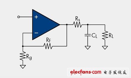
Figure 1: Add Rs at the output to improve stability.
Figure 2 shows a typical circuit configuration diagram for driving transmission cables (such as coaxial cables). Resistors Rs and RL should be equal to the characteristic impedance (Zo) of the cable, and capacitor C should be used to match the cable over a larger frequency range to compensate for the amplifier's output impedance that increases with increasing frequency.
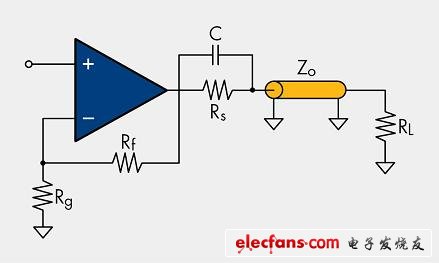
Figure 2: Typical circuit diagram of a drive cable or transmission line.
High-frequency amplifiers are easily affected by the distortion caused by the circuit layout. Even low-frequency amplifiers (such as audio amplifiers) have very strict distortion requirements. Total harmonic distortion (THD) is the main indicator of audio quality, so reducing the distortion caused by the layout is critical.
An important cause of distortion is the effect of ground current in the PCB. This effect comes from the current flowing into each power supply and each power supply bypass capacitor, which is proportional to the conductivity of the path. Each path has different conductivity, which leads to distortion. Because even if the material of the PCB itself is linear, the behavior of the circuit board will show "spatial nonlinearity". This is because the bypass capacitors are distributed at different positions on the circuit board, causing the ground current to flow into the bypass capacitors along different paths. The different paths cause the voltage at one end of the grounding resistance input through which the ground current flows to be affected, while the other end does not. The result is that the input signal voltage is adjusted unevenly, resulting in non-linearity. In this case, if one polarity is adjusted and the other is not, it will cause second harmonic distortion. In other words, if only one polarity of the sine wave is adjusted, the result will no longer be a sine wave, and the effect of this distortion is obvious. To avoid distortion, designers can use a common ground point and use a ground bypass capacitor at the output.
The main rule of high-frequency circuit board layout design is to make the high-frequency bypass capacitor as close as possible to the package power pin. However, experience has shown that slightly extending the connection trace of the high-frequency bypass capacitor can improve flatness and differential gain, thereby reducing distortion. Design rules are of course beneficial, and the practical experience of designers is also very useful, which can ensure that the rules are consistent with the actual.
When designing a video filter driver on a circuit board, it is important that the input coupling capacitors and termination resistors are placed close to the input pins to obtain the best signal integrity. Figure 3 shows a typical AC-coupled input configuration of a video filter / driver. In this configuration, a 0.1uF ceramic capacitor is used to AC-couple the input signal. If the input signal is not lower than the ground potential, the clamp circuit is not activated; but if the input signal is lower than the ground potential, the clamp circuit will set the minimum voltage of the synchronization terminal to be just below the ground potential. The input level set by the clamp circuit, combined with the internal DC offset, will keep the output signal within an acceptable range, around 250mV. This clamping feature also allows the DAC output referenced to ground to directly drive the DC-coupled input.
In order to obtain the highest output signal quality, the series termination resistors must be placed as close as possible to the output pins of the device. This will greatly reduce the influence of parasitic capacitance and parasitic inductance on the driver output. The distance from the device pin to the series termination resistor should not exceed 0.5 inches (see Figure 4). FIG. 5 is a typical schematic diagram of a video filter / driver as an output driver in a multimedia device. In the case shown in FIG. 5, the composite video signal terminal of the multimedia device is connected to the multimedia device, and the S-video output terminal is turned on. At this time, it is critical to place the series termination resistor close to the output pin of the device to minimize the effect of parasitic capacitance on the filter output driver, thereby avoiding oscillation at the output. Figure 6 shows Fairchild Semiconductor's FMS6346A video filter driver driving a 25pF load, and Figure 7 shows FMS6346A driving a 47pF capacitive load. This shows that the smaller the capacitance, the better the performance.
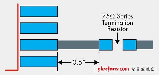
Figure 4: The distance from the device pin to the series termination resistor should not exceed 0.5 inches.
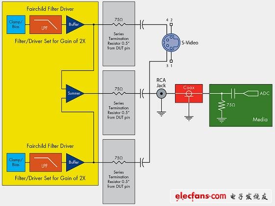
Figure 5: FMS6346A video filter output to S-Video.
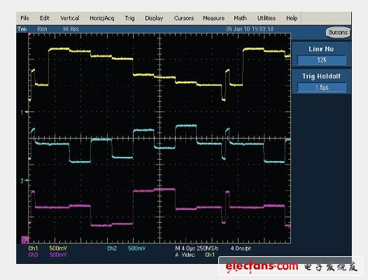
Figure 6: The FMS6346A video filter driver drives a 25pF load.
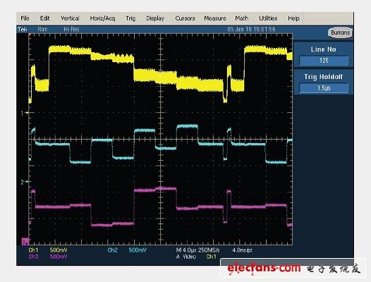
Figure 7: The FMS6346A drives a 47pF capacitive load.
Table Top Stove,Single Burner Gas Cooker,Stainless Steel Portable Stove,Indoor Portable Gas Stoves
Xunda Science & Technology Group Co.ltd , https://www.xundatec.com