
As FPGA chips get larger and system clocks increase, PCB board design and structural design become more difficult. As the rate increases, the signal integrity between boards becomes critical. If there are critical signals on the PCB, then Impedance matching is performed to avoid reflection and oscillation of the signal. Xilinx provides DCI with impedance matching inside the chip. The matching resistor is further connected to the chip, which can reduce components, save PDB board area, and is more convenient for routing.
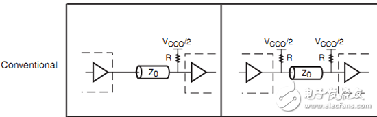
Traditional impedance matching is to terminate a resistor on the PCB. Ideally, the output impedance of the source is considered to be small, and the input impedance of the receiving end is considered to be very large. It can be ignored in the actual circuit. Only the traces on the PCB are considered, and the characteristic impedance of the PCB is seen from the receiving end. It should be equal to the termination resistor so that current flows from the source to the receiver without causing reflections.
Impedance Matching Impedance matching refers to an operating state in which the load impedance is matched with the internal impedance of the excitation source to obtain maximum power output. For circuits with different characteristics, the matching conditions are different. In a purely resistive circuit, when the load resistance is equal to the internal resistance of the excitation source, the output power is maximum. This operating state is called matching, otherwise it is called mismatch. When the impedance and load impedance of the excitation source contain reactance components, in order to maximize the power of the load, the load impedance and the internal resistance must satisfy the conjugate relationship, that is, the resistance components are equal, and the reactance components are only equal in value and opposite in sign. This matching condition is called a conjugate match.
In high-speed designs, the matching of impedance is related to the quality of the signal. The technique of impedance matching can be said to be rich and varied, but how to make a reasonable application in a specific system requires measuring various factors. For example, in our design in the system, many of them use the serial matching of the source segment. Why do you need to match and what kind of matching is used? For example, differential matching mostly uses parallel terminal matching; the clock uses series source matching.
The theoretical starting point of the series source matching matching series source matching is that a resistor R is connected in series between the source end of the signal and the transmission line under the condition that the signal source impedance is lower than the characteristic impedance of the transmission line, so that the output impedance of the source end and the characteristics of the transmission line are made. The impedance is matched to suppress re-reflection of the signal reflected from the load.
The signal transmission after serial terminal matching has the following characteristics:
1. Due to the action of the series matching resistor, the driving signal propagates to the load end with 50% of its amplitude.
2. The reflection coefficient of the signal at the load end is close to +1, so the amplitude of the reflected signal is close to 50% of the original signal amplitude.
3. The reflected signal is superimposed with the signal propagated at the source end, so that the signal received by the load end is approximately the same as the amplitude of the original signal.
4. The reflected signal of the load end propagates to the source end, and is absorbed by the matching resistor after reaching the source end.
5. After the reflected signal reaches the source, the source drive current drops to 0 until the next signal transmission.
Relative to series matching, the signal driver is not required to have a large current drive capability. The principle of selecting the matching value of the series source terminal is simple, that is, the sum of the matching resistance value and the output impedance of the driver is required to be equal to the characteristic impedance of the transmission line. The ideal signal driver's output impedance is zero, the actual driver always has a relatively small output impedance, and the output impedance may be different when the signal level changes. For example, a CMOS driver with a supply voltage of +4.5V has a typical output impedance of 37Ω at low level and a typical output impedance of 45Ω at high level [4]; the TTL driver and CMOS driver have the same output impedance as the signal The level changes as the level changes. Therefore, for TTL or CMOS circuits, it is impossible to have a very correct matching resistor, which can only be considered. The signal network of the chain topology is not suitable for series termination matching, and all loads must be connected to the end of the transmission line. It can be seen that there is a time when the load side signal amplitude is half of the original signal amplitude. Obviously, the signal is in an indeterminate logic state at this time, and the noise margin of the signal is very low.
Series matching is the most common method of terminal matching. It has the advantage of low power consumption, no additional DC load on the driver, no additional impedance between the signal and ground, and only one resistor component.
Parallel terminal matching
The theoretical starting point of parallel terminal matching is to eliminate the characteristic impedance of the transmission line by increasing the shunt resistance when the impedance of the signal source is small, so as to eliminate the reflection at the load end. The implementation form is divided into two forms: single resistance and double resistance.
The signal transmission after parallel terminal matching has the following characteristics:
1. The drive signal propagates along the transmission line at approximately full amplitude;
2. All reflections are absorbed by the matching resistors;
3. The amplitude of the signal received by the load is approximately the same as the amplitude of the signal sent by the source.
In the actual circuit system, the input impedance of the chip is very high, so for the single-resistance form, the parallel resistance value of the load terminal must be close to or equal to the characteristic impedance of the transmission line. Assuming that the characteristic impedance of the transmission line is 50 Ω, the R value is 50 Ω. If the signal's high level is 5V, the quiescent current of the signal will reach 100mA. Due to the small driving capability of typical TTL or CMOS circuits, this parallel matching of single resistors is rarely found in these circuits.
Parallel matching in the form of a double resistor, also known as the Thevenin termination, requires less current drive capability than a single resistor form. This is because the parallel values ​​of the two resistors match the characteristic impedance of the transmission line, and each resistor is larger than the characteristic impedance of the transmission line. Considering the driving capability of the chip, the choice of two resistor values ​​must follow three principles:
(1) The parallel value of the two resistors is equal to the characteristic impedance of the transmission line;
(2) The resistance value connected to the power supply should not be too small, so as to avoid excessive driving current when the signal is low;
(3) The resistance value connected to the ground should not be too small, so that the drive current is too large when the signal is high.
Conventional terminal matching requires that the resistor be as close as possible to the chip pin, which not only increases the difficulty of wiring the PCB, but also increases the number of components.
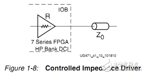
DCI technology According to the I/O level standard, DCI technology can control the output impedance of the driver, and can also add parallel terminals to the driver or receiver. The goal is to accurately match the characteristic impedance of the transmission line. The DCI technique calculates the internal impedance of the I/O based on the high precision reference resistors on the VRP and VRN. And it can continuously compensate for impedance changes caused by temperature and voltage changes.
For impedance controlled drivers, DCI matches the impedance to the external two reference resistors or to match half of the two reference resistors.
For parallel terminals, including transmitters and receivers, DCI technology brings the terminating resistor closer to the output driver or input buffer. For 7 Series FPGAs, DCI technology is only used in HP I/O banks and is not available for HR I/O banks. The Xilinx DCI uses two multiplexed pins to adjust the impedance of the driver or the parallel termination resistor. These two pins are VRN and VRP. VRN must be pulled up to VCCO through a reference resistor Rref, and VRP must be pulled down to ground through a reference resistor Rref. The resistance of this Rref is generally equal to the characteristic impedance of the PCB trace or twice the impedance.
To use DCI technology in your design, you need to meet the following conditions:
 The signal pin is at HP I/O BANK, and the standard for declaring the pin in the constraint is DCI.
上 Pull up a high-precision reference resistor on the VRN to Vcco.
接 Connect a high-precision reference resistor to the ground on the VRP.
 Both VRN and VRP are in the same HP BANK. Unless DCI iteration is used, DCI iteration only requires HP master BANK.
The DCI calculation can be reset by the DCIRESET primitive. By sending a RST high pulse to DCIRESET, DCI begins to calculate the impedance value and all I/Os that use DCI are not working until the LOCKED signal is pulled high.
Impedance Control Drivers For impedance control drivers, DCI offers two impedance matching types:
 and reference resistance are equal
 equals half of the reference resistance
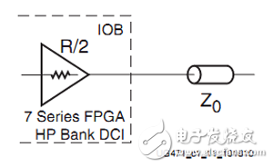
In this case, R must be equal to 2Z0, and the level standard should select DCI_DV2, such as the primitives of LVDCI_DV2_15 and LVDCI_DV2_18. This method is mainly used to reduce static power consumption.
Parallel termination (discrete resistance)
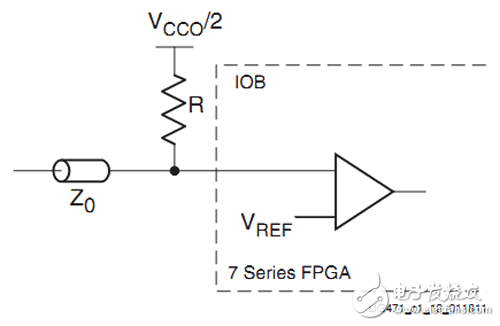
For parallel terminations, DCI uses a Thevenin equivalent circuit or a discrete resistor, using the Vcco/2 level.
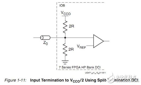
Its Thevenin equivalent circuit is as follows:
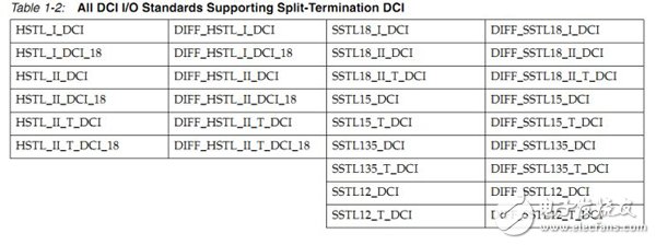
The DCI level standards for discrete resistors are as follows:
Tri-state DCI
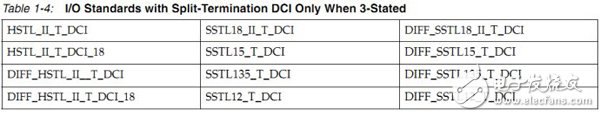
For some level standards, the first level standard such as SSTL and HSTL only supports one-way signals, while the second level standard supports both one-way and two-way signals. When the discrete terminal is in use, DCI only controls the impedance of the discrete terminal instead of the driver. The impedance, so for a two-way signal, when it acts as a driver, it needs to turn off the application of the discrete terminal. XILINX provides a DCI-T standard to meet this requirement, and only needs to change the corresponding level standard to this DCI-T. Tri-state DCI is only suitable for bidirectional signals. The level standards for tri-state DCI are as follows:
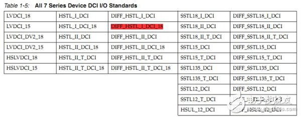
All level standards of DCI are listed below.
Screen Protector Cutting Machine
Tpu Hydrogel Cutting Plotter,Inteligent Screen Protector Cutter,Mobile Phone Cut Plotter,Screen Protector Cutter
Shenzhen TUOLI Electronic Technology Co., Ltd. , https://www.hydrogelprotectors.com