
Summary:
The wide input range of 90Vac to 305Vac for high-power PWM dimming LED street lighting is increasingly used, and the UCC28019A controller is very suitable for this application. However, the PFC inductor noise caused by the PWM dimming of the output load may be the main problem. In this article, we will analyze the root cause of this phenomenon based on the small signal model and propose solutions. In order to verify the effectiveness of this proposed solution, we use the UCC28019A average model and use experiments to test. It is proved that the experimental results are in good agreement with the analysis results and simulation results.
Key words:
UCC28019A, LED lighting, APFC, average model, load dynamics, simulation, noise issues
1 Introduction
The average current control of CCM operation is the most typical control scheme, which is widely used in high-power APFC converters, such as converters based on UC3854. Compared with peak current control, it has many advantages, such as: no need for external compensation slope, higher inspection current signal noise suppression and lower input current THD. However, the traditional CCM control scheme using multipliers inside the chip complicates the external current design. Recently, a new CCM (an 8-pin solution) using a 1-D control model, such as the TI UCC28019A controller, has become the first choice of engineers.
The UCC28019A controller uses the pulse and non-linear characteristics of the switch-mode converter to achieve immediate control of the rectified voltage or current average value. The purpose of designing this control scheme is to provide faster dynamic load response and better input disturbance rejection than other PFC controllers.
In actual engineering, most engineers are impressed by the high PF value of the wide input range UCC28019A controller and the excellent performance of the on-voltage boost without output overshoot. This advantage makes UCC28019A more suitable for this application than traditional BCM PFC controllers. This is especially true when more and more applications of high-power PWM dimming LED street lighting have a wide input range of 90 to 300Vac. However, when using dynamic response, its unique loop characteristics can cause visible noise issues.
In view of the above problems, the goal of this article is to introduce you a suitable solution that can improve this dynamic performance. First, Section 2 details this issue. In order to study the reason clearly, Section 3 analyzes the small signal of the current loop; based on this, the root cause is explained in detail, and a correct solution is proposed. In order to fully verify this solution, we also use the corresponding UCC28019A average model to verify the experimental tests and results in Section 4. Finally, combined with practical engineering applications, the article outlines some design techniques for this solution.
2. UCC28019A load dynamic visible noise description
Dynamic noise problems may occur in the following two situations:
· The load rise situation when the loop is not optimized (see Figure 1), at this time the peak inductor current of the PFC increases immediately, resulting in saturation of the ferrite sensor.
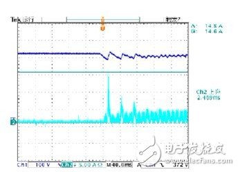
Figure 1 The load rise that saturates the PFC inductor
· Figure 2 shows the drop in load operation when the loop is not controlled during the OVP operation. In this process, the irregular frequency causes PFC high peak inductor current, which causes visible noise.
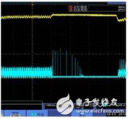
Figure 2 A load drop that causes saturation of the PFC inductor
Regarding LEDs—For outdoor applications, this phenomenon is suppressed because of the post-PWM load dimming requirements.
3. The root cause analysis based on the working principle of UCC28019A
Small signal modeling is the most practical method to study the stability of the converter control loop. This section focuses on the main small signal transfer function of the UCC28019A internal current loop, because the inductor current response under the voltage loop voltage disturbance is our main research goal.
3.1 Analyze the current noise of PFC inductor according to the change of Vcomp during the load rise of UCC28019A
As far as traditional PFC converters are concerned, the key to realizing power correction is to let the input current track the input voltage. [1] The document details the implementation of the 1-D control circuit. In order to study its small signal characteristics, in this section, we only introduce the realization of small signal transfer function. In fact, within UCC28019A, there are 2 loops: current loop and voltage loop.
After an in-depth study of the 1-D control scheme of the APFC converter, it is found that the 1-D functional equivalent circuit can be moved to the control module of the current loop. Please refer to the internal function module of [2]. Figure 3 shows the compensation current loop using the 1-D control scheme inside UCC28019A:
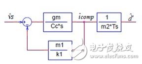
Figure 3 Cc-based current compensation loop
(  It is a small signal that disturbs the voltage of the PFC, Icomp, and 1-D current detection resistors; m1 and m2 are nonlinear gains, k1 is the internal controller constant, Cc is the compensation capacitor, and Ts is the switching time.
Transfer function of compensation current loop  The derivation is as follows:
As for power factor correction, the main problem is the working principle of tracking the input current of the input voltage. We know that in the low frequency range of 90 to 120 Hz, the input current always tracks the input voltage; therefore, the current loop is the only low-frequency characteristic problem. Like the UC3854, the power factor principle of the UCC28019A also combines the low frequency characteristics of the current loop. From equation (1), we can see that the low-frequency gain under stable operation is:
In addition, at low frequencies:
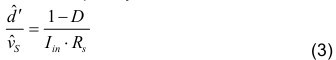
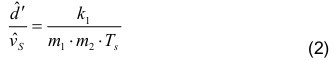
At low frequencies, combining equations (2) and (3), the result is:

See the principle of boost converter:
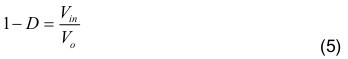
Finally, the input current formula that tracks the input voltage is derived as follows:
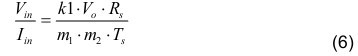
It indicates that PF has been reached. From the previous formula, the standard formula based on equation (1) is:

Vcomp's Iin disturbance can get:

among them 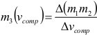 . The MathCAD expression is as follows:

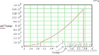
Figure 4 m3 (Vcomp) curve under Vcomp
From (8), we know that 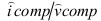 depending on
  The stable value of, which indicates that under certain stable operating conditions, the Iin current is still disturbed by these parameters. This also shows that the PFC current responds quickly after Vcomp changes rapidly.
From the previous analysis, we can draw the conclusion that if there is some small change in the PFC inductor current when a certain Vcomp disturbance is injected, it must also be reduced  Value. However, in the actual functional optimization design process, this is difficult to control. Therefore, the standard solution relies on the degree to which Vcomp changes when the entire voltage loop is closed.
3.2 UCC28019A Vcomp change root cause analysis during UCC28019A load rise
The UCC28019A product specification describes its voltage error amplifier as follows:

Figure 5 Internal principle of voltage loop
When more than 5% of the output voltage disturbance appears at the VSENSE input, the amplifier is out of linear operation. In the undervoltage state, the UVD function calls EDR, which immediately increases the voltage error amplifier transconductance from 42µs to 440µs. This high gain encourages the compensation capacitor to charge to a new operating level more quickly. This shows that EDR generates a large amount of Vcomp charge, which greatly improves Vcomp boost, especially when the output current increases sharply. Therefore, if the impact of Vcomp is reduced according to the EDR function requirements, the voltage loop response speed must be increased slightly to avoid the UVP point when possible. As shown in Figure 6, we must slightly reduce the response speed of the voltage feedback circuit (usually Ccv2) to make it slightly faster than the loop response time.
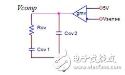
Figure 6 Voltage feedback compensation loop
3.3 UFC28019A controller PFC inductor current noise analysis during buck
In most cases, PFC inductive noise may appear during the PFC load drop. Experiments show that this inductive noise occurs when the output OVP is triggered. In addition, if OVP remains triggered, this noise may exist for a long period of time, especially when the load is switched to light load mode. Therefore, the noise will be closely related to the output OVP protection mode.
According to the product manual, UCC28019A has a very simple OVP protection mode-if OVP protection is triggered, it directly turns off the driver. But in the actual experiment, we found that the driver is abnormal in this state, and the inductor current also has some abnormally high peak electric shock.
Many experiments show that Vcomp declines very slowly with this process. If this buck time is shortened, the noise is reduced. Therefore, a good solution is to use some external method to quickly discharge the compensation capacitor when OVP is triggered. Once the Vcomp voltage drops, the output also deviates from the OVP level, and there is no longer a noise problem.
3.4 UCC28019A PFC inductor current noise solution during load drop
As analyzed in Section 3.3, there is a way to quickly reduce the Vcomp voltage. In some cases, this will not cause serious problems, because we have chosen a small value compensation capacitor, the noise is not so obvious. But in most cases, when the PCB layout is not ideal and the higher PF value is not reached, there is no room for optimization of the voltage compensation loop, but the noise reduction is still obvious; in this case, an external circuit is required To solve this problem.
The suggested solution is as follows:
For easy understanding, we use the standard OP and TL431 or TL103, the realization circuit shown in Figure 7.

Figure 7 Simple schematic diagram of the proposed solution compensation loop
Figure 8 shows the complete solution using TL103. Under normal circumstances, half of TL103 can be used for high temperature protection, which is required by safety standards in actual engineering.
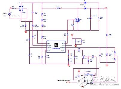
Figure 8: Complete solution to improve load dynamic performance using TL103
In actual design, the focus of this solution must meet the following requirements for the high tolerance of R1, R2, and TL103:

4. Use UCC28019A average model and actual experiment to verify the proposed solution
In order to verify the feasibility of the solution mentioned in the previous section, we established the UCC28019A average model and performed simulation. At the same time, manufacture experimental prototypes to verify the solutions.
The simulation model and experimental prototype are based on the parameters listed in Table 1.
Table 1 Prototype parameter list 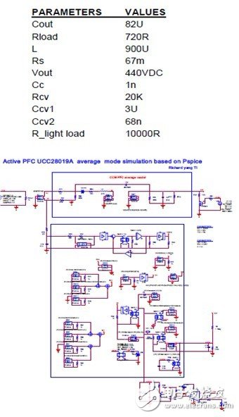
Figure 9 The average model of UCC28019A application
When the PFC changes from no-load to full-load transient, and the EDR is still operating in the PFC operating state, the peak current of the PFC inductor is inevitable; however, there is no inductor saturation problem and no visible noise. However, when the PFC transitions from full load to no-load transient, there is noise in the inductor. Figure 10 shows the simulation results of the initial application.
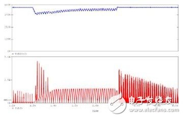
Figure 10 Simulation results of output and inductor current without TL103
From the previous simulation results, we know that when the PFC load drops, noise can be clearly observed. Now, Figure 9 describes this external TL103; Figure 11 shows the simulation results of the output voltage, inductor current, and OP output.

Figure 11 Simulation results of output, inductor current and TL103 output
From the simulation results shown in Figure 11, we can see that the noise has disappeared, and TL103 discharges the capacitor current of the voltage loop. Therefore, the output voltage can quickly enter the adjustment range. However, an important issue is that no-load power consumption requirements must not affect no-load operation.
In order to verify the actual working conditions, we made an experiment on the prototype. Figure 12 shows the measurement results based on the initial application; we can clearly see the presence of noise during the output load drop. However, with the improved solution, the noise disappeared (see Figure 13), which is the same as the simulation result.

Figure 12 TL103 output and PFC inductor current measurement results 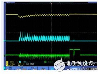
Figure 13 Measurement results of output, inductor current and TL103 output
5 Conclusion
Based on the initial UCC28019A application, this article details the root cause of noise problems during output load rise and fall. For PWM dimming LED street lighting applications, this is an urgent problem to be solved. We have proposed corresponding solutions for you, and verified their effectiveness through theoretical analysis and simulation as well as experimental measurements. The results show that they meet the requirements very well.
In short, we recommend that the external circuit of TL103 can optimize the voltage loop parameters to avoid load rising noise, and at the same time avoid load falling noise. Note that another part of TL103 can be used for high-temperature protection in actual engineering, which means that this suggested external circuit has great use value.
The Touch Monitor is a product developed and designed by ourselves. It has been sold for more than 6 years and has exceeded 160,000 units. At present, it is running very well. It mainly customizes different touch technologies, different sizes, different interfaces, connecting cables and power supply parts to meet the needs of guests. We provide customers with the choice of Resistive Touch Screen, Capacitive Touch Screen, Infrared Touch Screen and nano touch foil, and customize various interfaces for customers, such as: VGA, DVI, HDMI, DP and so on. It is mainly used in banks, hospitals, government units, airports, railway stations, supermarkets, real estate and other places.
Product show:


Touch Monitor
Touch Screen Monitor,Multi Touch Display Monitor,Outdoor Touch Screen Monitor,Waterproof Touch Monitor,Commercial Touch Screen Monitor,KTV Touch Screen Monitor
ShenZhen GreenTouch Technology Co.,Ltd , https://www.bbstouch.com