
**First, the Difference Between Via and Pad**
**1. Via**
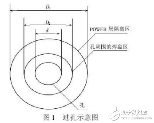
A via is a conductive hole used to connect different layers of a PCB. There are three main types: through-hole, blind via, and buried via.
- **Through-hole via**: This type goes all the way from the top layer to the bottom layer, allowing electrical connection between all layers. It is commonly used for internal connections or as a mounting hole for components.
- **Blind via**: This connects the outer layer to one or more inner layers but does not go all the way through the board. Only one side of the hole is visible.
- **Buried via**: This connects two or more inner layers and is completely hidden within the board, not visible from either the top or bottom.
Vias are primarily used for electrical connections between layers and are generally not used for soldering components. They consist of a drilled hole and a surrounding copper pad. The size of a via is typically small, while the holes used for component mounting (pads) are larger.
In simple terms, pads are larger holes designed for soldering components, while vias are smaller holes used to connect different layers electrically.
From a technical perspective:
- A **via** is a conductive hole that connects multiple layers of a PCB, with electrical continuity but no soldering function.
- A **drilled hole** (not always a via) is a mechanical hole used for assembly purposes, which may not have electrical properties.
- A **pad** is a copper area on the PCB surface, either plated or gold-plated, used to secure electronic components. It has electrical continuity and allows for soldering.
**2. Pad**
A pad is a copper area on the PCB, used to attach components. There are two main types:
- **Through-hole pad (pin pad)**: This has a hole in the center and is used for inserting component leads.
- **Surface mount pad (SMD pad)**: This has no hole and is used for soldering surface-mount components directly onto the board.
Pads are essential for both electrical connection and mechanical fixation. The size of a pad must be large enough to allow component pins to pass through, and the surface must be free of solder mask to ensure proper soldering.
**Key Differences**
- Vias are used for inter-layer electrical connections, while pads are used for attaching components.
- Vias are usually smaller and do not require solder mask coverage, whereas pads must be exposed for soldering.
- Pads have a larger aperture to accommodate component leads, while vias are designed to be as small as possible for space efficiency.
**Second, the Difference in Manufacturing Processes**
- In via design, the actual hole size after processing is usually about 0.1mm smaller than the designed size due to plating and drilling tolerances. For example, a 0.5mm via may end up being 0.4mm.
- For pads, the hole size increases by approximately 0.15mm during drilling, and after copper plating, it becomes slightly larger—about 0.05mm more than the design. So, a 0.5mm pad might end up being 0.55mm in the final product.
- Vias may be covered with solder mask in some PCB processes, which can prevent soldering and make testing difficult.
- The minimum width of a via's solder ring is typically 0.15mm (in standard processes), ensuring reliable copper plating.
- For pads, the minimum width of the solder ring is 0.20mm, to ensure strong adhesion and good soldering performance.
Understanding these differences helps in designing better PCBs and avoiding common manufacturing issues. Whether you're working on a simple prototype or a complex multilayer board, knowing how vias and pads function is crucial for success.
Packages For Consumer Electronics,Dual Inline Housing,Complex Integrated Circuit,Integrated Circuit Package
Shaanxi Xinlong Metal Electro-mechanical Co., Ltd. , https://www.cnxlalloys.com