
Abstract: This article introduces the principle of a zero-IF receiver, and the design and implementation of a zero-IF receiver based on the high-performance modem chip HFA3787.
Introduction As we all know, the working process of the traditional "superheterodyne" wireless receiver is as follows: the weak high-frequency radio signal must pass through the mixing circuit of one or more stages to remove interference from other channels and obtain sufficient gain, and finally completed Demodulate and retrieve the required information.
In order to overcome the defects of image interference and the need for high-Q filters in "superheterodyne" wireless receivers, the concept of a zero-IF receiver has been proposed. This structure, called Direct-Conversion or Zero-IF, has the following advantages: (1) The IF frequency is zero, and there is no image interference problem; (2) The channel selection is carried out at a low frequency. It is very convenient to use integrated circuits to digitize signals.
However, the zero-IF receiver also has obstacles that are not easy to eliminate, such as DC offset and low-frequency noise, so someone has proposed a dual-conversion wih wideband Fisrt IF receiver. This receiver converts the high-frequency signal to a higher intermediate frequency during the first frequency conversion, and the output of the second frequency conversion is zero intermediate frequency. This article takes the structure of this kind of zero-IF receiver. Figure 1 shows its working principle.
HFA3783 chip function and structure
HFA3783 is a comprehensive chip launched by Intersil for half-duplex wireless applications. It contains all necessary functional modules for quadrature modulation and I / Q demodulation. Its intermediate frequency receiving AGC amplifier has a frequency response range of 600 MHz and a voltage gain of 70 dB, and has a gain control range of more than 70 dB; the transmit output also has a gain control range of 70 dB. Its receiving and transmitting intermediate frequency can share a differential matching filter network to reduce the number of filtering devices necessary in a single intermediate frequency half-duplex transmitter. In the receiving mode, there are functions such as DC offset correction circuit and intermediate frequency level detection. Its internal mixer is driven by a broadband orthogonal LO generator, the IF frequency setting and PLL loop synchronization parameters are controlled by a 3-wire serial interface, it only requires a low-level external VCO and a frequency up to 50 MHz reference source. Its function module is shown in Figure 2.
Its main characteristics are as follows:
It integrates all the functions of intermediate frequency transmission and reception. The wide amplitude orthogonal frequency range is 70 to 600MHz. The intermediate frequency AGC dynamic range is 69dB. It has a DC-coupled baseband interface and a receive DC offset correction loop. It is controlled by a 3-wire serial interface. PLL loop synchronization, local oscillator drive level is -15dBm, transmit / receive function switching <1μs, with power management / waiting mode and single voltage (2.7V ~ 3.3V) power supply.

Figure 1 Schematic diagram of double-conversion wide-IF receiver

Figure 2 HFA3783 function module diagram
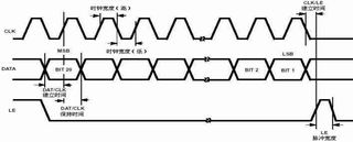
Figure 3 Synchronous serial timing diagram

Figure 4 Circuit block diagram of a class zero IF receiver
Parameter setting and register function
Since HFA3783 is a half-duplex mode, it requires input pins PE1, PE2 and the lowest bit M (0) of register M to define the working state of transmission / reception. Its truth table is shown in Table 1.
HFA3783 has 5 internal function registers, all of which are set through a 3-wire serial interface. The three input pins are: clock (CLK), data (DATA), and latch (LE). The input timing is shown in the figure. 3 shown.
When the data input is full of 20 bits, a latch signal is input. The HFA3783 judges which register to set by comparing the lower 2 bits of data. The specific settings are shown in Table 2.
Among them, R is the frequency division ratio of the reference source, A / B and M (2) are the VCO frequency division coefficient. HFA3783 controls the VCO tuning voltage by comparing the divided reference frequency REF / R with the divided VCO / [P * B + A], and finally makes the PLL loop lock to the frequency set by the user.
The value of the C register determines the frequency and time for correcting the DC offset level in the receive mode. The formula for calculating the correction time is:
Calibration time = 22 & TImes;
Among them fREFIN is MHz level.
M is the working mode register, it must be set first, followed by other registers.
The circuit implementation of the quasi-zero IF receiver The RF section adopts the traditional structure, so we will not repeat them here. The circuit block diagram is shown in Figure 4.
Here, FPGA is used to configure parameters of HFA3783, and FPGA and DSP are used to co-process baseband data. In baseband processing, the low-level signal preprocessing algorithm processes a large amount of data and requires high processing speed, but the operation structure is relatively simple, so it is suitable for hardware implementation with FPGA. In contrast, the amount of data processed by the high-level processing algorithm is relatively small, but the control structure of the algorithm is complex, and it is suitable for being implemented by a DSP chip with high operation speed, flexible addressing mode, and powerful communication mechanism.
Conclusion In addition to the modulation and demodulation circuits, the HFA3783 also integrates intermediate frequency amplification, AGC, baseband low-pass filtering and other circuits. In this way, the intermediate frequency circuit of the zero-IF receiver requires only a few devices, and it is also debugged. It is more convenient; and HFA3783 can also provide a 1.2V reference level for A / D sampling to improve the accuracy of A / D sampling.
However, we found that there are several problems that must be noted during hardware debugging:
* The frequency division factor of the VCO and reference frequency is a contradiction with the PLL loop phase noise of the local oscillator: if the frequency division factor is selected small, the PLL loop may not lock properly; if the frequency division factor is selected large, the phase noise of the PLL loop is also Increased accordingly, this requires specific compromise to choose a compromise.
* Impedance matching needs careful consideration. At the intermediate frequency input and output of HFA3783, a filter matching network can be shared, and its impedance is 250W.
* The baseband of the HFA3783 requires a bias voltage of 1.3V, otherwise the intermediate frequency will not work properly.
The scheme of quasi-IF receiver introduced in this paper has been successfully applied in a certain type of spread spectrum unit, and all performance indexes have reached the requirements.
Plasma Photocatalysis Gas Purifier
Industrial Air Purifiers,Waste Gas Purification,Plasma Photocatalytic Gas Purifier,Plasma Photocatalysis Gas Purifier
Dongguan V1 Environmental Technology Co., Ltd. , https://www.v1airpurifier.com