
Design of Video Image Acquisition System Based on TMS320F2812
The fast-growing automotive industry provides a broad application market for in-vehicle electronic products, such as in-vehicle "infrared surveillance", "reversing radar" and other video surveillance equipment, which brings convenience and safety to the driver. These monitoring devices are inseparable from video image acquisition, and the key link of video image acquisition is the AD conversion of video signals. The traditional video image acquisition system generally uses a special image acquisition chip, such as the SAA7110 video decoding chip, to automatically complete the image acquisition; the disadvantage is that the circuit is complicated and the cost is high, it is inconvenient to program and upgrade the software, and the accuracy of the image acquisition And the speed is also restricted, and the adaptability to non-standard video signals is not good.
This design uses DSP's on-chip ADC to achieve image acquisition. It does not require a professional video decoding chip. Although it cannot complete automatic image acquisition, it has the characteristics of simple circuit, low cost, easy maintenance and upgrade. More importantly, it can be programmed by software to adapt to the collection of different standard video signals. When using DSP and CPLD to build a data acquisition system, there is no need to connect a professional image acquisition chip, which avoids complicated hardware design and provides sufficient processing power. This design adopts TI's TMS320F2812 chip to collect images, and builds TMS320C6416t to process images to achieve DSP-based video image acquisition.
System scheme of video image acquisition
Video image acquisition includes a video preprocessing circuit and an A / D conversion circuit, and its structural block diagram is shown in Figure 1.
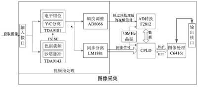
Figure 1 Block diagram of video acquisition
Firstly, the synchronization of the acquired image signal is separated, and the separated synchronization signal is connected to the CPLD. After preprocessing such as level clamping and amplitude adjustment, the video signal is connected to the ADC input of F2812.
F2812 outputs the result of its on-chip ADC to CPLD through XINTF, and CPLD transmits the video brightness signal to the image processor C6416t through HPI for image processing according to the timing relationship of the separated synchronization signal. Among them, the main design of this article is the front-end image acquisition part, users can replace the image processor according to their needs to meet different image processing requirements.
1 Video preprocessing
The analog video signal includes video brightness signal, video chrominance signal, and video synchronization signal. The peak-to-peak value of the video signal is 1V, and its synchronization signal level is lower than zero level. The ADC range used by F2812 is 0 ~ 3V, so before video conversion, Y / C separation, synchronous separation, level clamping, amplitude amplification and other pre-processing are required.
â‘ Y / C separation and level clamping
This system uses Philips' TDA9181 and TDA9143 chips for Y / C separation. TDA9181 is a multi-standard dynamic comb filter, consisting of delay, adder, subtractor, and band-pass filter. It supports PAL B, G, H, D, I, M, N, and NTSC M standard combing. Y / C separation is performed for the video signal of its related system. TDA9181 can also level clamp the input signal.
TDA9143 is a PAL / NTSC / SECAM decoder controlled by I2C bus, which can provide TDA9181 with sandcastle pulse signal and color subcarrier frequency signal required for Y / C separation.
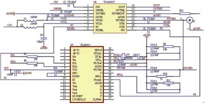
Figure 2 Y / C separation principle diagram
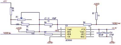
Figure 3 AD8066 video buffer schematic

Figure 4 Synchronous separation
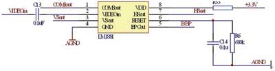
Figure 5 LM1881 separation principle diagram
The schematic diagram of TDA9181 and TDA9143 interface is shown in Figure 2.
â‘¡Video buffer
Because the peak-to-peak value of the video signal is 1V, and the F2812 ADC range is 0 ~ 3V, so in order to better video sampling, the video signal needs to be amplified 3 times.
The AD8066 used in the system is a single-channel and dual-channel operational amplifier with high-voltage, high-speed, low-power, and high-current rail-to-rail output. The differential gain error and differential phase error are 0.01% and 0.02%, respectively, and the 7MHz bandwidth gain is uniform. The performance is 0.1dB, which is very suitable for video buffering applications.
The schematic diagram of the AD8066 used as a video buffer is shown in Figure 3.
â‘¢ synchronous separation
The synchronous separation adopts LM1881 chip of NS Company. LM1881 can separate various synchronization signals from PAL, NTSC and SECAM video signals with peak-to-peak values ​​of 0.5 to 2V, as shown in Figure 4 (a: composite video signal, b: composite synchronization signal, c: field synchronization signal, d: Parity field signal, e: burst / back shoulder signal). In addition, LM1881 can also be applied to the synchronous separation of non-standard video signals, the principle is shown in Figure 5.
2 Video A / D converter
TMS320F2812 is a 32-bit fixed-point programmable processor chip with a maximum frequency of 150MHz, which can be easily connected to other processors. The maximum sampling bandwidth of the on-chip 12-bit ADC can reach 12.5MHz, and it has a FIFO equivalent to 16 levels, so that the on-chip ADC can achieve The upper limit working rate can achieve 1 data every 80ns. In addition, TMS320F2812 can be easily programmed by software to adapt to video signals of different standards, so F2812 is used for AD conversion.
The working flow chart using cascade, continuous automatic sorting mode is shown in Figure 6.

Figure 6 AD conversion work flow chart
3 Video image processing
This system is designed to use CPLD external expansion TMS320C6416t to process images, users can replace the image processor according to their needs to achieve the required processing effect.
Image Acquisition
1 Acquisition process â‘ After the Y / C separation and level clamping of the PAL / NTSC analog video signal output by the camera through TDA9181 and TDA9143, all the way to TMS320F2812 becomes a digital signal, and the other way to the LM1881 to separate the synchronization signal.
â‘¡ Transfer the image data collected by F2812 to CPLD through its XINTF; separate the parity field signal and composite synchronization signal from LM1881 to CPLD for logic control.
â‘¢ According to the odd-even field signal and the composite synchronization signal, the CPLD decides whether to acquire the odd-field image or the even-field image, or to acquire a complete frame of image. (Users can also use their own expanded image processor to determine the frame number of the image.)
2 lines and field processing â‘ When the field synchronization signal arrives, CPLD decides whether to collect the odd field image or even field image, or to collect a complete image according to the parity field signal; when the composite synchronization signal arrives, CPLD determines which line. CPLD will control the acquisition of F2812 according to these logic timings, and provide synchronous timing to the externally expanded image processor.
â‘¡Users can also process these synchronization signals according to their own needs, such as using an externally expanded image processor instead of CPLD to determine the line and field of the image.
System performance
Only when the speed and accuracy of AD acquisition meet the requirements of video image changes can video images be collected in real time. The standard PAL analog video signal has 625 scanning lines per field, the actual transmitted image per frame is 575 lines, the field frequency is 50 Hz, the frame frequency is 25 frames per second, and the signal change frequency per second is 5.52 MHz, that is, the image The signal bandwidth is 5.52MHz. According to the sampling theorem, the AD sampling bandwidth is at least 11MHz. The on-chip AD converter of the TMS320F2812 has a maximum sampling bandwidth of up to 12.5MHz, so it fully meets the requirements for collecting video signals in terms of speed. Similarly, the F2812's video AD conversion accuracy is 12 bits, and users can also write correction algorithms on the F2812's ADC module to continuously improve the ADC's conversion accuracy.
application
The system platform can be used for video image collection and data parameter collection of various formats, and can be made into a video capture card and a data capture card. The video capture card can be used for on-board video surveillance, such as target recognition and reversing radar.
Connect the infrared image sensor to the input end of the video capture card, and connect the display device to the output interface, it can be used for night infrared monitoring. Users can easily program the image processor (such as C6416t) for target acquisition and recognition. For example, when the car is driving at night and there is an unknown obstacle in front of it, the infrared monitor will give an alarm in advance and display the target on the monitor to remind the driver.
Connect an ordinary photoelectric camera to the input end of the video capture card, which can be used for reversing video surveillance. In this way, the driver does not have to turn around and turn his head to reversing the car. He only needs to look at the video monitor on the side to reverse the car.
The system platform can also be used for the collection of multiple data parameters. Different data sensors are connected to the input of the video capture card, which can be used for data parameter monitoring of industrial automation and automobiles. For example, whether the tire pressure of the car is normal, whether the air quality in the car is up to standard, whether the driving speed is too fast, whether the water temperature is too high, and whether the remaining fuel is too low, etc., can be collected through the data parameters, to Remind the driver.
Conclusion
This system does not require a special ADC chip, and a single DSP can realize video image and data collection; and it can facilitate software programming of F2812 to continuously improve the quality of image and data collection; in addition, CPLD provides a rich external expansion interface, users You can easily replace your own image processor, which provides convenience for future image data processing.
The design of Led Down Light is more beautiful and light, and the ight is not exposed, no glare. LED downlight is recyclable, environmentally friendly and not fragile, Down lights are generally used in shopping malls, offices, factories, hospitals and other indoor lighting, easy to install. LED down light inherited the advantages of all the traditional downlight, lowheat, long life, lowcosts.

Led Down Light
Led Down Light,Led Slim Down Light,Led Recessed Down Light,Down Light Led
Zhongshan Laidi Lighting Co.,LTD , http://www.idealightgroup.com