
MOSFETs are widely used in switching power supplies because of their low on-resistance, high switching speed, and other advantages. The MOSFET driver often selects the appropriate circuit based on the parameters of the power supply IC and MOSFET. To discuss drive circuit for a switching power MOSFET below.
When using MOSFETs to design switching power supplies, most people consider the MOSFET's on-resistance, maximum voltage, and maximum current. But many times only consider these factors, such circuits may work, but not a good design. In more detail, the MOSFET should also consider its parasitic parameters. For a certain MOSFET, its drive circuit, the peak current of the drive pin output, the rate of rise, etc., will affect the MOSFET's switching performance.
When the power supply IC and the MOS transistor are selected, it is particularly important to select an appropriate driver circuit to connect the power supply IC and the MOS transistor.
A good MOSFET drive circuit has the following requirements:
(1) When the switch tube is turned on instantaneously, the drive circuit should be able to provide enough charging current to quickly raise the voltage between the gate and the source of the MOSFET to the required value to ensure that the switch tube can be turned on quickly and there is no high-frequency oscillation at the rising edge.
(2) The driver circuit ensures that the voltage between the gate and the source of the MOSFET remains stable and reliable when the switch is on.
(3) The off-time transient drive circuit can provide a path with the lowest possible impedance for rapid discharge of the capacitor voltage between the gate and the source of the MOSFET, ensuring that the switch can be quickly turned off.
(4) The drive circuit has a simple, reliable structure and low losses.
(5) Apply isolation as appropriate.
The following describes the MOSFET drive circuits commonly used in several module power supplies.
1, power IC directly drives MOSFET
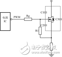
Figure 1 IC Direct Drive MOSFET
The direct drive of the power IC is the most commonly used drive method, and it is also the simplest drive method. Using this drive method, several parameters and the influence of these parameters should be paid attention to. First, look at the power IC manual, the maximum driving peak current, because different chips, driving ability is often not the same. Second, look at the MOSFET's parasitic capacitance, as shown in Figure 1, C1, C2 value. If the values ​​of C1 and C2 are relatively large, the required energy for turning on the MOS transistor is relatively large. If the power IC does not have a relatively large driving peak current, the conduction speed of the tube is relatively slow. If the drive capability is insufficient, high-frequency oscillation may occur at the rising edge. Even if Rg in Figure 1 is reduced, it will not solve the problem! Factors such as IC drive capability, MOS parasitic capacitance, and MOS transistor switching speed all affect the selection of the drive resistor value, so Rg cannot be infinitely reduced.
2. When the power IC driver capacity is insufficient
If the parasitic capacitance of the MOS transistor is relatively large and the internal driving capability of the power supply IC is insufficient, it is necessary to enhance the driving capability of the driver circuit. A totem pole circuit is often used to increase the power IC driving capability, and the circuit thereof is shown in a dashed box in FIG.
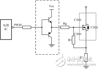
Figure 2 Totem pole drive MOS
The role of this drive circuit is to increase the current supply capability and quickly complete the charging process for the gate input capacitive charge. This topology increases the time required to turn on, but reduces the turn-off time, allows the switch to turn on quickly, and avoid high-frequency oscillations on the rising edge.
3, drive circuit to accelerate the MOS transistor off time
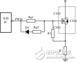
Figure 3 Accelerated MOS Shutdown
The off-time transient drive circuit can provide a path with the lowest possible impedance for rapid discharge of the voltage between the MOSFET gate and source, ensuring that the switch can be quickly turned off. In order to quickly discharge the capacitor voltage between the gate and the source, a resistor and a diode are often connected in parallel on the driving resistor, as shown in FIG. 3 , where D1 is a fast recovery diode. This reduces the turn-off time while reducing the loss at turn-off. Rg2 is to prevent excessive current when turning off, and burns the power IC.
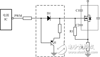
Figure 4 Improved Accelerated MOS Shutdown
The totem pole circuit introduced in the second point also accelerates the shutdown. When the driving capability of the power supply IC is sufficient, the improvement of the circuit in FIG. 2 can speed up the MOS transistor turn-off time, and the circuit shown in FIG. 4 can be obtained. It is common to use a triode to drain the gate-to-source capacitance voltage. If there is no resistance at the emitter of Q1, when the PNP transistor is turned on, the capacitor between the gate and source is shorted to discharge the charge in the shortest time, minimizing the cross-over loss at turn-off. Compared with the topology of Fig. 3, there is a benefit that the current does not pass through the power IC when the charge on the capacitor between the gate and the source is discharged, thereby improving the reliability.
4, drive circuit to accelerate MOS tube off time
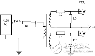
Figure 5 Isolated drive
In order to satisfy the driving of the high-side MOS transistor as shown in Fig. 5, the transformer driver is often used, and sometimes the transformer driver is used to satisfy the safety isolation. The purpose of R1 is to suppress the parasitic inductance on the PCB board and C1 form an LC oscillation. The purpose of C1 is to separate the DC, through the AC, and also to prevent the core saturation.
In addition to the above drive circuits, there are many other forms of drive circuits. For a variety of drive circuits and no drive circuit is the best, only with the specific application, select the most suitable drive. In the design of power supply, there are several angles to consider how to design the drive circuit of the MOS transistor. If a finished power supply is used, no matter whether it is a module power supply, an ordinary switching power supply, or a power adapter, this part of the work is generally completed by the power supply design manufacturer.
The isolated power supply module independently developed and produced by Zhiyuan Electronics has been accumulated in the industry for nearly 20 years. Currently, the product has a wide input voltage range and is isolated from 1000VDC, 1500VDC, 3000VDC, and 6000VDC series. The package is available in various forms and is compatible with the international standard SIP. DIP and other packages. At the same time, Zhiyuan Electronics has built a first-class testing laboratory in the industry to ensure the performance of its power supply products. It is equipped with the most advanced and complete testing equipment. The entire series of isolated DC-DC power supplies passes a complete EMC test, and the electrostatic immunity is as high as 4KV and surge resistance. The interference can reach as high as 2KV, and it can be applied to most complex and harsh industrial sites, providing users with a stable and reliable power isolation solution.
In addition to the above drive circuits, there are many other forms of drive circuits. For a variety of drive circuits and no drive circuit is the best, only with the specific application, select the most suitable drive.
However, due to technical and cost reasons, it is not widely used. In recent years, RFID technology has developed by leaps and bounds. With the development of large-scale integrated circuit and network communication technology, RFID technology has entered the commercial application field, and began to develop from the initial low frequency (125kHz) and high frequency (13.56mhz) to uHF (860 ~ 960MHz) and microwave. RFID technology has become one of the most promising information technologies in the new era because of its unique advantages showing great development potential and application space. In both low and high frequency bands, China has independently developed RFID chips in accordance with ISO14443 A, B and ISO15693 standards, which have been successfully applied in major projects such as city bus all-in-one card and second-generation resident ID card. However, in the uHF and microwave field, China started late, technology and products are still relatively short. In this context, this paper studies the design of 915MHz rf card reader. The system can be applied to vehicle monitoring, remote control, telemetry, access control system, identity identification, non-contact radio frequency smart card, wireless 485/232 data communication, safety and fire prevention and other fields.
915MHZ Rubber Antenna,915MHZ Antenna with magnetic base,915MHZ fiberglass antenna
Yetnorson Antenna Co., Ltd. , https://www.xhlantenna.com