
One of the best ways to reduce electromagnetic interference (EMI) in PCB design is to use operational amplifiers flexibly. Unfortunately, in many applications, this effect of the op amp is often overlooked. This may be due to the prejudice that "op amps are susceptible to EMI and additional measures must be taken to increase their immunity to noise."
Automotive, industrial, medical, and many other applications often use sensitive analog circuits that must perform their function in their work environment while maintaining immunity to noise interference. Many of these disturbances are caused by "noise" circuits located on the same printed circuit board (PCB), which couple to the cable interface on the PCB and its circuitry.
One of the best ways to reduce electromagnetic interference (EMI) in PCB design is to use operational amplifiers (“op ampsâ€) flexibly. Unfortunately, in many applications, this effect of the op amp is often overlooked. This may be due to the prejudice that "op amps are susceptible to EMI and additional measures must be taken to increase their immunity to noise." Although many previously produced devices do, designers may not realize that recent op amps generally have better EMI immunity than previous generations. Designers may also not understand or consider the key advantages that op amp circuits can provide to reduce noise in their system and PCB designs. This article reviews the sources of EMI and discusses op amp characteristics that help to reduce near-field EMI on sensitive PCB designs.
EMI source, victim circuit and coupling mechanism
EMI is interference caused by an electrical noise source that inadvertently and often undesirably strikes a secondary electrical circuit. In all cases, the interfering noise signal is one of voltage, current, and electromagnetic radiation, or the noise source is coupled to the victim circuit in some combination of these three forms.
EMI is not limited to radio frequency interference (RFI). There are strong EMI sources in the frequency bands below the RF in the “lower†frequency range, such as switching regulators, LED circuits, and motor drivers operating in the tens to hundreds of kilohertz range. 60Hz line circuit noise is another example. The noise source transmits noise to the victim circuit through one or four possible coupling mechanisms. Three of the four methods are considered near-field coupling, including: conductive coupling, electric field coupling, and magnetic field coupling. The fourth mechanism is far-field radiative coupling in which electromagnetic energy is radiated at multiple wavelengths.
Differential mode noise active filtering
Active op amp filters can significantly reduce EMI and noise on the PCB within the circuit bandwidth, but in many designs they are underutilized. The desired differential mode (DM) signal can be band limited, and unwanted DM noise is filtered out. Figure 1 shows the DM noise coupled into the input signal through a parasitic capacitance (CP). The combined signal and noise are received by a first-order active low-pass filter. The low-pass cut-off frequency of the differential opamp circuit is set to be only higher than the desired signal bandwidth determined by R2 and C1.
The higher frequencies are attenuated by 20 dB/decade. If higher attenuation is required, high-order active filters (for example, -40 or -60 dB/decade) can be used.
It is recommended to use < 1% tolerance resistors. Also, capacitors with excellent temperature coefficient (NPO, COG) and 5% (or < 5%) tolerance can achieve optimal filter performance.
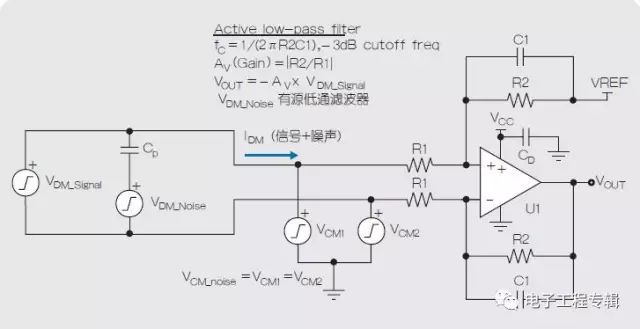
Figure 1: DM and CM input noise applied to active opamp filters
Reduce input common-mode noise
In Figure 1, the common mode (CM) noise source also generates noise at the input of the circuit. CM noise can be described as a common (or the same) noise voltage at the two op amp inputs and is not part of the expected differential mode signal that the op amp is trying to measure or regulate. CM noise can occur in many ways. One example is a system where the ground reference voltage of one circuit is at a different voltage potential than the second circuit it interfaces with. The difference in "ground" voltage can be a millivolt or several volts level and can also occur at many different frequencies. These differences in voltage can cause unexpected voltage drops and can interfere with the flow of current through the connected circuit.
Cars, airplanes and large buildings with numerous circuits are often susceptible to this type of interference.
A key advantage of op amps is their differential input stage architecture and the ability to suppress CM noise when configured as a differential amplifier. The common mode rejection ratio (CMRR) is specified for each op amp, but the total CMRR of the circuit must also include the effects of the input and feedback resistors. The change in resistance strongly influences the CMRR. Therefore, a matching resistor with a tolerance of 0.1%, 0.01% or better is required to achieve the CMRR required for the application. Although using an external resistor can achieve good performance, using an instrument with an internal trim resistor or a differential amplifier is also an option. For example, the INA188 is an instrumentation amplifier with internal trimming resistor and 104dB high CMRR.
In Figure 1, if the noise is within the effective bandwidth of the circuit, the CM noise (VCM_noise = VCM1 = VCM2) can be suppressed by the CMRR of the op amp circuit. The level of suppression depends on the exact matching resistor chosen by R2 / R1. Equation 1 can be used to determine the CMRRTOTAL, which includes the tolerances (RTOL) specified in the data sheet and the effects of the op amp CMRR. For example, if the op amp data sheet specifies its CMRR (dB) = 90dB, (1/CMRRAMP) = 0.00003. In many circuits, the resistor tolerance becomes the main limiting factor for achieving the target CMRRTOTAL.
Equation 1 is derived from the CMRR equation of the ideal op amp described in reference 1, where the CMRRAMP term is assumed to be very large (infinity). For a perfect op amp, the (1/CMRRAMP) term is zero and CMRRTOTAL is determined only by the resistance and the AV. CMRRTOTAL can be converted to dB using Equation 2.
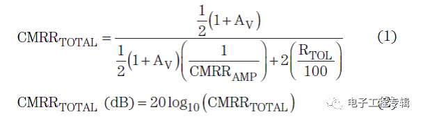
Where AV = closed-loop gain of the op amp, RTOL = tolerance % of R1 and R2 (for example, 0.1%, 0.01%, 0.001%), CMRRAMP = CMRR in decimal format (not dB) in the datasheet specification.
Improve immunity to RFI and other high frequency EMI
As mentioned earlier, active filtering and CMRR can reliably reduce circuit noise within device band limits, including DM and CM EMI up to the MHz range. However, exposure to RFI noise above the expected operating frequency range may result in non-linear behavior of the device. The op amp is most susceptible to RFI due to its high-impedance differential input stage because DM and CM RFI noise can be rectified by an internal diode (formed by a pn junction on silicon). This rectification produces a small DC voltage or offset that is amplified and may exhibit an erroneous DC offset at the output.
Depending on the accuracy and sensitivity of the system, this may result in poor circuit performance or behavior.
Fortunately, using one of two methods can improve the op amp's immunity to RFI (or reduce susceptibility). The first and best option is to use EMI-hardened op amps, which include an internal input filter that can suppress noise in the tens of megahertz up to 1000 megahertz range.
TI currently offers more than 80 types of EMI hardened devices that can be found by searching TI's "EMI Hardened".
The second option is to add an external EMI/RFI filter to the input of the op amp. This may be the only choice if the design requires the use of a device that does not include an internal EMI filter.
Figure 2 shows a standard differential amplifier configuration using an external DM and CM filter that targets a higher EMI frequency.
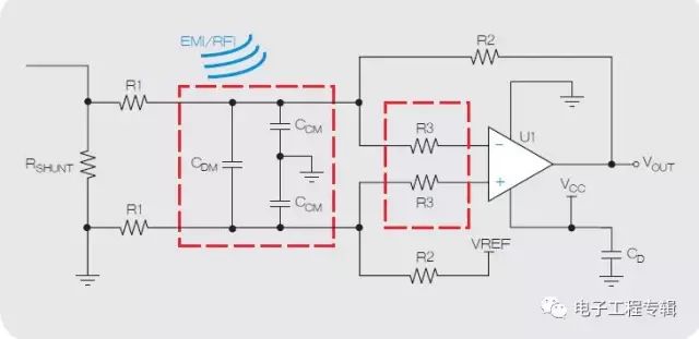
Figure 2: Passive EMI/RFI input filter improves high frequency immunity
Without the input filter, the circuit gain is |R2/R1|. If a passive input filter is added, an R3 resistor is usually needed to prevent the CDM capacitor from reducing the phase margin of the amplifier. The DM low-pass filter consists of an R1 resistor, CDM, and two CCM capacitors.
The CM low-pass filter uses an R1 resistor and two CCM capacitors.
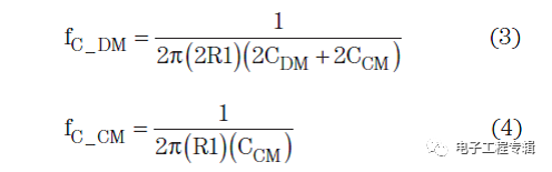
The equation for the -3dB cutoff frequency of the DM and CM filters (fC_DM and fC_CM) is as follows. The fC_DM is set to a frequency above the desired bandwidth of the op amp circuit, and the CDM is usually determined first. The CCM capacitor is then chosen to be at least ten times smaller than the CDM to minimize its effect on fC_DM, and also because the CCM capacitor is targeted for higher frequencies. Therefore, fC_CM will be set to a frequency higher than fC_DM. Please note that the EMI hardened device can be used to replace the device enclosed by the red wire frame, simplifying the design.
Low output impedance reduces interference
Another important characteristic of an op amp is its extremely low output impedance, which is typically a few ohms or less in most configurations. To understand how to reduce EMI, consider how EMI affects low-impedance and high-impedance circuits.
The diagram in Figure 3 shows two circuits. The first is the input audio circuit of an analog-to-digital converter (ADC), which includes a 1VP-P, a 2 kHz sine wave (VS1), a 600 Ω source impedance (RS1), and a 20 kΩ load impedance (RL1). Source impedances such as 600Ω are common in audio applications such as microphones; high input impedances such as 20k are common in audio ADCs. The second circuit is a 100 kHz clock source that drives the 3.3V clock signal (VS2). The series termination resistor is 22Ω (RS2) and the load impedance is 500 kΩ (RL2). A high impedance load represents the digital input of another device.
In real systems, I2C serial bus clocks in the range of 100 to 400 kHz are common in audio ADCs and circuits. Although the I2C clock is usually driven in a burst (discontinuous) manner, this simulation shows the possible effects when the clock is driven. In high-density audio and infotainment PCB designs, clock traces near the sensitive audio traces do appear. Capacitive coupling can occur with just a few pF of parasitic PCB capacitance, and clock noise current can be injected into the victim audio signal. FIG. 3 is a simulation example using only a 1 pF parasitic capacitance.
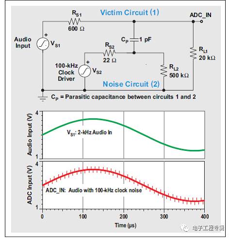
Figure 3: Clock Noise Source and Audio Perturbation Circuit
Audio input: Audio input Victim circuit: Clocked circuit Clock driver: Clock driver Noise circuit: Noise circuit ADC Input: ADC input Parasitic capacitance between circuits 1 and 2: Parasitic capacitance between circuit 1 and circuit 2 Audio with 100kHz clock noise: Audio Time with 100kHz Clock Noise: Time
How does the audio circuit reduce noise? It turns out that reducing the impedance of a victim circuit is one way to reduce its sensitivity to coupled noise. For circuits with higher source impedance (>50Ω), the coupling noise can be reduced by minimizing the source impedance associated with the circuit load. In FIG. 4, an in-phase configured OPA 350 is added to the circuit to buffer the signal and isolate the source impedance from the load. Compared with 600Ω, the output impedance of the op amp is very low, which significantly reduces the clock noise.
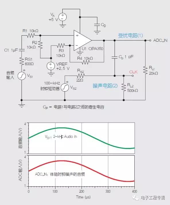
Figure 4: Op Amp Circuit to Reduce Clock Source EMI
Don't forget the importance of decoupling
Adding a decoupling capacitor at the power supply pin is useful for filtering high frequency EMI noise and enhancing the immunity of the op amp circuit. All diagrams in this article show that the out-coupling capacitor CD is part of the circuit. Although exploration of decoupling problems will soon enter deepwater areas, there are some good “rules of thumb†that apply to any design. In particular, choose a capacitor with the following characteristics: (a) Very good temperature coefficient, such as X7R, NPO, or COG(b) Extremely low equivalent series inductance (ESL) (c) Lowest impedance in the desired spectral range (d ) Capacitance values ​​in the range of 1 to 100 nF are usually very awesome, but the above criteria (b) and (c) are more important than the capacitance value (d).
The location of the capacitors and the trace connections are as important as the selected capacitors. Place the capacitor as close as possible to the power pin. The connection between the capacitor and the PCB power/ground should be as short as possible, using short traces or vias.
in conclusion
The op amp can help reduce near-field EMI on the PCB and enhance system design. Here are some points to consider for any design:
Use a carefully selected active filter configuration to reduce the input DM noise of the cable/circuit (Figure 1).
By selecting an op amp with high CMRR and using precision matched resistors, the input CM noise of the cable/circuit is reduced (Figure 1, Equations 1, 2).
Immune to high-frequency EMI or RFI (DM/CM noise) immunity by selecting EMI hardened devices or using external passive EMI/RFI filters (Figure 2).
When driving signals to other circuits on the PCB, use the low impedance of the op amp output to reduce the coupling noise.
Finally, power supply noise is reduced by applying appropriate decoupling strategies to the op amp and all other circuits.
Three Phase Portable EV Charger
Three Phase Portable Ev Charger,Ev Home Charger,Portable Electric Charger,Electric Charger
Yangzhou JERI New Energy Co., Ltd. , https://www.jrevcharging.com