
Precision power control of the MAX3740 laser driver
| Abstract: This article describes and analyzes three circuits that can accurately control the laser power of the MAX3740 laser driver. The schematic, simulation results, and their respective advantages and disadvantages of each circuit are introduced. The output power level of the MAX3740 VCSEL laser driver can be controlled by software. This can be achieved by using it in conjunction with the DS1859 digital potentiometer, but it requires high skill. This article introduces the challenges in the design, and presents two schemes that use DS1859 and a discrete resistor to control the output power (Scheme # 1 and Scheme # 2), and a new scheme that uses a single op amp to solve the shortcomings of all discrete components. (Scheme # 3). At the same time, the simulation results of the relationship between photodiode current and potentiometer resistance in each scheme are also given. Finally, the advantages and disadvantages of each scheme are summarized. For a specific application, the best circuit depends on the designer's needs. The design considerations include the photodiode current that meets the laser power level requirements, the adjustment range, and the required resolution. Designers can use the information in this article to determine the best solution for a particular application. Challenge MAX3740 data sheet requires a resistor between the reference pin (REF) and the power monitoring photodiode (MD) to set the photodiode current. The power control loop controls the output intensity of the laser diode based on this photodiode current to meet the average optical power requirement. The problem is that the rated voltage of MD is 1.6V, while the rated voltage of REF is 1.8V. Only 0.2V across the resistor sets the photodiode current. The minimum resistance that a digital potentiometer like DS1859 can achieve is 1K. The corresponding maximum current is 200µA. You can use a fixed resistor to increase the current, but it cannot solve the limited adjustment range, nonlinearity, and poor resolution at high currents. Another challenge with the DS1859 is that the voltage range between the MAX3740's MD and REF pins is very large. Although the difference between the two points is stable at 0.2V, the common-mode voltage can vary up to ± 0.5V. A large change in the MD's voltage to ground means that the current defined by its resistance to ground will have an equally large change. Solution # 1 In this solution, a DS1859 variable resistor and a fixed resistance of 806Ω are connected in parallel between REF and MD, as shown in Figure 1. The fixed resistor current is 0.2V / 806 = 248µA, and the variable resistor current range is 0.2V / 50K (DS1859 maximum) = 4µA to 0.2V / 1K (DS1859 minimum) = 200µA. The sum of the current of the fixed resistance and the variable resistance determines the current flowing through the photodiode. This method can provide a high-resolution nonlinear response at low currents. It is not affected by changes in MD voltage. 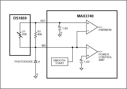 Figure 1. Schematic diagram of scenario # 1 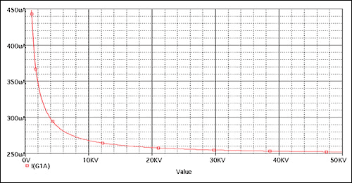 Figure 2. Simulation result of scheme # 1 (X-axis is the DS1859 resistance value in ohms) 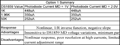 Figure 3. Summary of Scheme # 1 Scheme # 2 In this scheme, the DS1859 is connected between MD and ground, and a fixed 243Ω resistor is placed between REF and MD, as shown in Figure 4. The current of the fixed resistor is 0.2V / 243 = 823µA. The current range of the variable resistor is: 1.6V (MD rated voltage) / 50K (DS1859 maximum) = 32µA to 1.6V (MD rated voltage) / 1K (DS1859 minimum) = 1600µA. The current of the photodiode is equal to the current of the fixed resistance minus the current of the variable resistance. This method provides higher resolution at high currents. But the current value strongly depends on the voltage change of MD. Note that the photodiode current may show a negative value when the variable resistance value is low. Figure 5 shows the change in photodiode current when the MD and REF values ​​change within ± 5V. 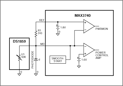 Figure 4. Schematic diagram of scenario # 2 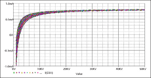 Figure 5. Simulation results when the MD and REF values ​​in Scheme # 2 vary within ± 0.5V (X-axis is the DS1859 resistance value in ohms) 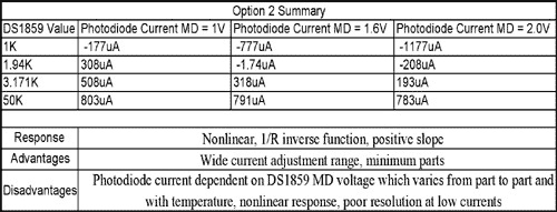 Figure 6. Summary of Solution # 2 Solution # 3 This solution uses a small form factor (SC70 package) op amp, MAX4245, connected between the REF and MD pins, as shown in Figure 5. When using the same power supply as the DS1859 and MAX3740, the output voltage VO of the op amp is proportional to the MD, REF-MD values, and the DS1859 resistance. This makes the current through R2 proportional to the voltage difference between VO and MD. In order to counteract the impact of the MD pin voltage change, the current through R2 depends only on REF-MD, a stable 0.2V, and the resistance of the DS1859. The current through the photodiode is equal to the current through R1 (803µA) + the current through R2. The photodiode current is a linear function of the resistance of the potentiometer. This circuit can use any resistance potentiometer, and can provide any range of current. The only limitation is the current drive capability of the MAX4245 op amp. The output voltage (VO) of the op amp can be calculated by the following formula. Make sure that the VO voltage does not exceed the maximum output swing of the op amp. VO = REF *-(DS1859 / R3) + MD * (1 + DS1859 / R3) VO = -REF * DS1859 / R3 + MD + MD * DS1859 / R3 VO = MD + (MD-REF) * DS1859 / R3 VO = MD-0.2V * DS1859 / R3 VO = 1.0V (minimum)-0.2V * 1K (DS1859 minimum) / 10K = 0.98V VO = 1.0V (minimum)-0.2V * 50K (DS1859 maximum) / 10K = 0V VO = 2.0V (maximum)-0.2V * 1K (DS1859 minimum) / 10K = 1.98V VO = 2.0V (maximum)-0.2V * 50K (DS1859 maximum) / 10K = 1.0V The current value through R2 can be calculated by the following formula. I (R2) = (VO-MD) / R2 I (R2) = VO / R2-MD / R2 I (R2) = (MD-0.2V * DS1859 / R3) / R2-MD / R2 I (R2) = MD / R2-0.2V * DS1859 / R2 * R3-MD / R2 I (R2) = -0.2V * DS1859 / R2 * R3 I (R2) = -DS1859 / 62,000,000 I (R2) = -1K (DS1859 minimum) / 62,000,000 = -16µA I (R2) = -50K (DS1859 max) / 62,000,000 = -806µA 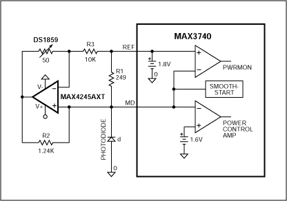 Figure 7. Schematic diagram of scenario # 3 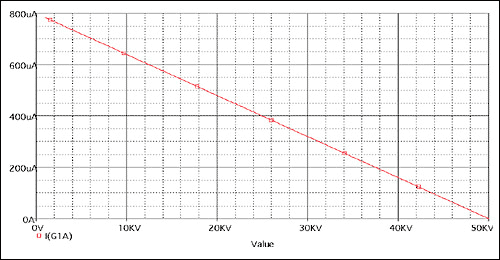 Figure 8. Simulation results of scheme # 3 (X-axis is the DS1859 resistance value in ohms) 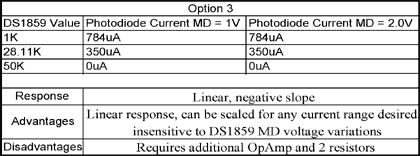 Figure 9. Summary of Scheme # 3 This article introduces three schemes for controlling the power level of the MAX3740 laser driver. Schemes # 1 and # 2 are very simple, but traded for reduced performance. Solution # 3 obtained a very good linear control by adding an op amp, and was not sensitive to device changes. Designers can choose the best solution according to their needs. |
This one is Cyclone Vacuum Cleaner. It is turely a cyclone Vacuum Cleaner always with strong power. It s cleaning efficiency is always high. Its filter system is 5 stages,so it can use for a long time. We have gotten international patent for the cyclone system used on our vacuum cleaner. So you can use more reliablely. In a word,iIt is worth to own this vacuum cleaner.


Cyclone Vacuum Cleaner
Cyclone Vacuum Cleaner, Dual Cyclone Vacuum Cleaner, Cyclone Bagless Vacuum Cleaner
Ningbo ChinaClean Household Appliances Manufacture Co., Ltd. , https://www.chinaclean-elec.com