
This application note also applies to the following Dallas Semiconductor framers and Dallas Semiconductor LIU:
| DS3 / E3 Framer | DescripTIon |
| DS3141 | Single-Port Framer |
| DS3142 | Dual-Port Framer |
| DS3143 | Triple-Port Framer |
| DS3146 | 6-Port Framer |
| DS3148 | 8-Port Framer |
| DS31412 | 12-Port Framer |
| DS3 / E3 / STS-1 LIU | DescripTIon |
| DS3151 | Single-Port LIU |
| DS3152 | Dual-Port LIU |
| DS3153 | Triple-Port LIU |
Receive negative data input / receive line code violation input (RNEG / RLCV): If BIN = 0 in the MC1 register, the LIU interface is in bipolar mode (POS / NEG). In this mode, the framer inputs a serial data stream in alternating sign inversion (AMI) format with the clock. RPOS = 1 on the external LIU indicates that a positive pulse was received on the line, and RNEG = 1 on the LIU indicates that a negative pulse was received on the line. If BIN = 1, the framer is in binary (NRZ) LIU interface mode. In this mode, the framer inputs the serial data stream in binary format with the clock at the RNRZ pin, and the line code violation at the RLCV pin.
Receive clock input (RCLK): RCLK is used to send data from RPOS / RNEG (bipolar LIU interface mode) or RNRZ (binary LIU interface mode) to the receive framer. If RCLKI = 0 in the MC5 register, data enters the framer on the rising edge of RCLK. If RCLKI = 1, data enters the framer on the falling edge of RCLK. RCLK obtained from LIU usually has an accuracy within ± 20ppm, but the framer can also receive up to 52MHz gap clock on RCLK, such as those from ICs that map DS3 and E3 to SONET / SDH or demap Clock.
DS3144 sends formatted LIU interface pins to send positive data output / transmit NRZ data output (TPOS / TNRZ): if BIN = 0 in the MC1 register, the LIU interface is in bipolar (POS / NEG) mode. In this mode, the transmit formatter outputs the serial data stream in AMI format. TPOS = 1 tells the external LIU to drive a positive pulse on the line, and TNEG = 1 tells the LIU to drive a negative pulse on the line. If BIN = 1, the LIU interface is in binary (NRZ) mode. In this mode, the transmit formatter outputs the serial data stream in a binary format on the TNRZ pin. TNRZ = 1 means a 1 in the data stream, and TNRZ = 0 means 0.Send negative data output (TNEG): If BIN = 0 in the MC1 register, the LIU interface is in bipolar (POS / NEG) mode. In this mode, the send formatter outputs the serial data stream in AMI format. TPOS = 1 tells the external LIU to drive a positive pulse on the line, and TNEG = 1 tells the LIU to drive a negative pulse on the line. If BIN = 1, the LIU interface is in binary (NRZ) mode. In this mode, the transmit formatter outputs the serial data stream in binary format on the TNRZ pin, and TNEG is set low.
Transmit clock output (TCLK): TCLK is used to send the framer to output clock data from TPOS / TNEG (bipolar LIU interface mode) or TNRZ (binary LIU interface mode). If TCLKI = 0 in the MC5 register, data is sent out of the formatter on the rising edge of TCLK. If TCLKI = 1, data is output on the falling edge of TCLK. TCLK is usually the buffered output of TICLK (inverted). When the line loopback or load loopback is activated, TCLK is the buffered output of RCLK (inverting is optional). When there is no clock signal on TICLK and MC1: LOTCMC = 1, TCLK is the RCLK buffer output (inverting can be selected).
DS3154 Receive-LIU Framer Interface Pin Receiver Positive AMI / Receiver Data (RPOS / RDAT): When the receiver is configured as a bipolar interface (RBIN = 0), every time a positive AMI pulse RPOS is received High pulse. When the receiver is configured as a binary interface (RBIN = 1), RDAT outputs decoded binary data. RPOS / RDAT is refreshed on the falling edge of RCLK (RCINV = 0) or the rising edge of RCLK (RCINV = 1).Receiver negative AMI / line code violation (RNEG / RLCV): When the receiver is configured as a bipolar interface (RBIN = 0), RNEG is a high pulse every time a negative AMI pulse is received. When the receiver is configured as a binary interface (RBIN = 1), RLCV generates a high pulse to indicate a code violation. RNEG / RLCV is refreshed on the falling edge of RCLK (RCINV = 0) or on the rising edge of RCLK (RCINV = 1).
Receiver clock (RCLK): The recovered clock is output on the RCLK pin. The recovered data is output from the RPOS / RDAT and RNEG / RLCV pins on the falling edge of RCLK (RCINV = 0) or the rising edge of RCLK (RCINV = 1). During signal loss (RLOS = 0), the RCLK output signal is obtained from the LIU master clock.
DS3154 transmits -LIU framer interface pin transmitter positive AMI / transmitter data (TPOS / TDAT): when the transmitter is configured as a bipolar interface (TBIN = 0), when TPOS is high, a positive pulse is sent on the line. When the transmitter is configured as a binary interface (TBIN = 1), the data on TDAT is sent after being encoded by B3ZS or HDB3. TPOS / TDAT samples on the rising edge of TCLK (TCINV = 0) or the falling edge of TCLK (TCINV = 1).Transmitter negative AMI (TNEG): When the transmitter is configured as a bipolar interface (TBIN = 0), when TNEG is high, a negative pulse is transmitted on the line. When the transmitter is configured as a binary interface (TBIN = 1), TNEG is ignored and set high or low. TNEG samples on the rising edge of TCLK (TCINV = 0) or the falling edge of TCLK (TCINV = 1).
Transmitter clock (TCLK): DS3 (44.736MHz _20ppm), E3 (34.368MHz _20ppm) or STS-1 (51.840MHz _20ppm) clock acts on this signal. The data to be transmitted is shifted into the device from the TPOS / TDAT and TNEG pins on the rising edge of TCLK (TCINV = 0) or the falling edge of TCLK (TCINV = 1).
DS3144 and DS3154 registers required for the interface: Table 1 shows the DS3144 registers corresponding to the highest level of configuration, control, and each framer state including reset, clock, pin control, and line interface functions.Table 1. DS3144 line interface register map
| ADDR. | REGISTER | BIT 7 | BIT 6 | BIT 5 | BIT 4 | BIT 3 | BIT 2 | BIT 1 | BIT 0 |
| 01h | MC1 | LOTCMC | ZCSD | BIN | MECU | AECU | TUA1 | DISABLE | RST |
| 02h | MC2 | OSTCS | TCCLK | N / A | N / A | N / A | DLB | LLB | PLB |
| 03h | MC3 | TDENMS | TSOFC | TOHENI | TOHI | TSOFI | TICLKI | TDATI | TDENI |
| 04h | MC4 | RDENMS | ROOFI | RLOSI | RDATH | RSOFI | ROCLKI | RDATI | RDENI |
| 05h | MC5 | RNEGI | RPOSI | RCLKI | TNEGH | TPOSH | TNEGI | TPOSI | TCLKI |
| 06h | ISR1 | N / A | N / A | N / A | N / A | INT4 | INT3 | INT2 | INT1 |
| 08h | MSR | LORC | LOTC | T3E3 | FEAC | HDLC | BERT | COVF | N / A |
| 09h | MSRL | LORCL | LOTCL | N / A | N / A | N / A | N / A | COVFL | OSTL |
| OAh | MSRIE | LORCIE | LOTCIE | T3E3IE | FEACIE | HDLCIE | BERTIE | COVFIE | OSTIE |
Note: The underlined bits are read-only bits. The bits marked N / A are undefined. Undefined bits are reserved for future function upgrades and must be written as logic 0 and ignored when read.
Table 2 shows the DS3144 DS3 / E3 framer register. In this register address map, the underlined bits are read-only bits. The bits marked N / A are undefined. Undefined bits are reserved for future function upgrades and must be written as logic 0 and ignored when read.
The registers in Table 2 correspond to the highest-level configuration, control, and status of each framer in DS3 and E3 modes.
Table 2. DS3144 DS3 / E3 Framer Register Map
| ADDR. | REGISTER | BIT 7 | BIT 6 | BIT 5 | BIT 4 | BIT 3 | BIT 2 | BIT 1 | BIT 0 |
| 10 | T3E3CR1 | E3SnC1 | E3SnC0 | T3IDLE | TRAI | TAIS | TPT | CBEN | DS3M |
| 11 | T3E3CR2 | FRESYNC | N / A | TFEBE | AFEBED | ECC | FECC1 | FECC0 | E3CVE |
| 12 | T3E3EIC | MEIMS | FBEIC1 | FBEIC0 | FBEI | T3CPBEI | T3PBEI | EXZI | BPVI |
| 18 | T3E3SR | N / A | N / A | SEF | T3IDLE | RAI | AIS | OOF | LOS |
| 19 | T3E3SRL | COFAL | N / A | SEFL | T3IDLEL | RAIL | AISL | OOFL | LOSL |
| 1A | T3E3SRIE | COFAIE | N / A | SEFIE | T3IDLEIE | RAIIE | AISIE | OOFIE | LOSIE |
| 1B | T3E3IR | RUA1 | T3AIC | E3Sn | N / A | EXZL | MBEL | FBEL | ZSCDL |
| 20 | BPVCR1 | BPV7 | BPV6 | BPV5 | BPV4 | BPV3 | BPV2 | BPV1 | BPV0 |
| twenty one | BPVCR2 | BPV15 | BPV14 | BPV13 | BPV12 | BPV11 | BPV10 | BPV9 | BPV8 |
| twenty two | EXZCR1 | EXZ7 | EXZ6 | EXZ5 | EXZ4 | EXZ3 | EXZ2 | EXZ1 | EXZ0 |
| twenty three | EXZCR2 | EXZ15 | EXZ14 | EXZ13 | EXZ12 | EXZ11 | EXZ10 | EXZ9 | EXZ8 |
| twenty four | FECR1 | FE7 | FE6 | FE5 | FE4 | FE3 | FE2 | FE1 | FE0 |
| 25 | FECR2 | FE15 | FE14 | FE13 | FE12 | FE11 | FE10 | FE9 | FE8 |
| 26 | PCR1 | PE7 | PE6 | PE5 | PE4 | PE3 | PE2 | PE1 | PE0 |
| 27 | PCR2 | PE15 | PE14 | PE13 | PE12 | PE11 | PE10 | PE9 | PE8 |
| 28 | CPCR1 | CPE7 | CPE6 | CPE5 | CPE4 | CPE3 | CPE2 | CPE1 | CPE0 |
| 29 | CPCR2 | CPE15 | CPE14 | CPE13 | CPE12 | CPE11 | CPE10 | CPE9 | CPE8 |
| 2A | FEBECR1 | FEBE7 | FEBE6 | FEBE5 | FEBE4 | FEBE3 | FEBE2 | FEBE1 | FEBE0 |
| 2B | FEBECR2 | FEBE15 | FEBE14 | FEBE13 | FEBE12 | FEBE11 | FEBE10 | FEBE9 | FEBE8 |
DS3154 can work in hardware mode or CPU bus mode.
In hardware mode, all configurations can be done by setting the input pin high or low. All status information is reflected on the status output pin. The internal registers are not accessible in hardware mode. When the HW pin is pulled high (HW = 1), the device is configured for hardware mode.
In CPU bus mode, the configuration pins and status pins in most hardware modes are reassigned to address, data, and control lines, which interface with the 8-bit microprocessor bus. When the HW pin is set low (HW = 0), the device is configured for CPU bus mode.
In addition to the HW pin, configuration pins and status pins in hardware mode have corresponding register bits in CPU bus mode. The hardware mode pins and CPU bus mode register bits have the same name and function, the difference is that all register bits are active high. Table 3 is the DS3154 register map, which can be used to interface with the DS3144.
Table 3. DS3154 register map
| ADDR. | REGISTER | BIT 7 | BIT 6 | BIT 5 | BIT 4 | BIT 3 | BIT 2 | BIT 1 | BIT 0 |
| 00h | GCR1 | E3M | STS | LLB | RLB | TDSA | TDSB | - | RST |
| 01h | TCR1 | - | TBIN | TCINV | TJA | TPD | TTS | TLBO | - |
| 02h | RCR1 | ITU | RBIN | RCINV | RJA | RPD | RTS | RMON | RCVUD |
| 03h | SR1 | - | - | TDM | PRBS | - | - | RLOL | RLOS |
| 04h | SRL1 | - | - | TDML | PRBSL | PBERL | RCVL | RLOLL | RLOSL |
| 05h | SRIE1 | - | - | TDMIE | PRBSIE | PBERIE | RCVIE | RLOLIE | RLOSIE |
| 06h | RCVL1 | RCV [7] | RCV [6] | RCV [5] | RCV [4] | RCV [3] | RCV [2] | RCV [1] | RCV [0] |
| 07h | RCVH1 | RCV [15] | RCV [14] | RCV [13] | RCV [12] | RCV [11] | RCV [10] | RCV [9] | RCV [8] |
| O8h-0Fh | TEST | - | - | - | - | - | - | - | - |
After reset, the default DS3144 LIU interface format is a bipolar (POS / NEG) format with B3ZS / HDB3 encoding and decoding. In order to change the working format of the framer after reset to the binary (NRZ) format without B3ZS / HDB3 encoding and decoding (encoding and decoding are turned off in the framer, but should be turned on in the LIU), BIN in the MC1 register The bit needs to be set to 1.
Framer interface format and DS3154 B3ZS / HDB3 decoder data can be output in binary or bipolar format. In order to select the bipolar interface format, the RBIN pin needs to be set low in hardware mode. In CPU bus mode, the RBIN configuration bit needs to be cleared.In the bipolar format, the B3ZS / HDB3 decoder is turned off, and the recovered data is buffered and output in RPOS and RNEG. RPOS = 1 indicates that a positive pulse is received, and RNEG = 1 indicates that a negative pulse is received.
In the bipolar interface format, the receiver simply passes the received data without BPV or EXZ check. In order to select the binary interface format, the RBIN pin should be set high in hardware mode. In CPU bus mode, the RBIN configuration bit needs to be set to 1.
In binary format, the B3ZS / HBD3 decoder is turned on to decode the recovered data and output as a binary number on the RDAT pin. The RLCV pin can mark a code violation.
To support the interface with various adjacent components, the polarity of RCLK can be reversed. Normally, data is output from the RPOS / RDAT and RNEG / RLCV pins on the falling edge of RCLK. To output data from these pins on the rising edge of RCLK, the RCINV pin needs to be set high in hardware mode, or the RCINV configuration bit is set to 1 in CPU bus mode.
The RCLK, RPOS / RDAT, and RNEG / RLCV pins have a three-state mode that supports protection switches and redundant LIU applications. This tri-state performance supports two or more LIU lines or together, one of which is selected by the system processor for efficient operation. To make RCLK, RPOS / RDAT, and RNEG / RLCV tri-stated, set the RTS pin high or set the RTS configuration bit. Figure 1 shows the functional block diagram of the Dallas Semiconductor framer DS3144 and Dallas Semiconductor LIU DS3154.
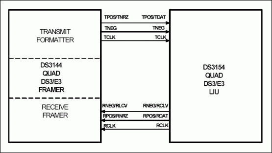
Figure 1. Functional block diagram of framer and LIU
For more questions about the connection and / or interface connection between Dallas Semiconductor framer and LIU, please email var name = "telecom.support @"; var domain = "dalsemi.com"; document.write ("" + name + domain + ""); telecom. Contact the Dallas Semiconductor Telecommunications Application Support Group (English only) or call 972-371-6555 (English only).
Carbon Fiber Products Include : Carbon Fiber Boom from ø6mm to ø80mm Thickness from 0.5mm to 10mm ,Carbon Fiber Plate,Carbon Fiber Board thickness from 0.5mm to 10mm, Carbon Fiber Shell
Carbon Fiber Boom,Carbon Fiber Plate,Carbon Fiber Board,Carbon Fiber Shell
shenzhen GC Electronics Co.,Ltd. , https://www.jmrdrone.com