
Compared with traditional liquid crystal display (LCD) screens, organic light-emitting diodes (OLEDs, also known as organic electro-laser displays), which are recognized by the industry as the next-generation display technology, are not only solid-state, light, active, high-quality, Low power consumption, etc., can also be used to try to break through the traditional screen form such as transparency, reel, folding, curved surface, etc. OLED is the future display technology direction that the industry pays attention to, but compared with the small and medium size OLED screen using low temperature polysilicon technology, application Large-size OLED screens with oxide technology have encountered many technical difficulties in the popularization. Currently, due to some key technologies, low cost and low yield, OLED panel scale application and large-scale industrialization still have a long process. .
Products with OLED large screenPanels, organic material coatings and packaging are the three major indicators for the mass production of OLED large-screen products. Due to the difficulty in breaking through the bottleneck of developing large-scale equipment, the low-temperature polysilicon (LTPS) panel process is difficult to cross the 5.5-generation OLED panel production line because this technology is The red, green and blue organic illuminants are horizontally vapor-deposited on the glass panel. Since the metal mask must be used during the evaporation, the metal mask is sunk and mixed due to gravity when the large panel is made, so Suitable for large size and high resolution. In view of this, amorphous germanium (a-Si) and oxide thin film transistor (Oxide TFT) panels have become the technology development choice. However, the electronic movement speed of the former is too slow, which will reduce the dynamic display response speed of the OLED panel. Therefore, the latter has become the first choice for technology research and development, but this technology has been slow. Fortunately, the oxide thin film transistor panel material and process are similar to amorphous germanium, so some amorphous germanium has process equipment that can be used by oxide thin film transistors.
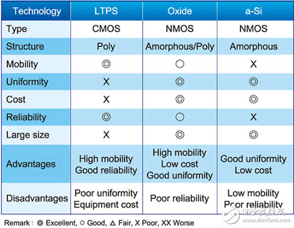
Panel technology comparison table
Common oxide semiconductors such as indium gallium zinc oxide (InGaZnO) are new materials with an electron mobility of up to 10 cm 2 / VS, which are dozens of times more than conventional amorphous germanium (1 cm 2 / VS). . Amorphous structure can achieve good uniformity in large size, suitable for large-size panels, achieving high definition, low power consumption, low leakage, but its reliability is poor and PMOS manufacturing process is difficult. It is a technology that needs to be improved. The former is an important key that must be overcome in the commercialization of mass production. The latter can be overcome by the compensation circuit (CompensaTIon Circuit).
Products with OLED transparent screenCommon oxide thin film transistor device structures mainly include Coplanar, Island Stop/Etch Stop Layer (IS/ESL) and Back Channel Etch (BCE). The coplanar structure is simple in process, but because the oxide semiconductor layer is required to climb the source metal, it is easy to cause electrical characteristics and contact problems, and the reliability is not good. As for the back channel etching and etching barrier layer structure, it is more advantageous in terms of component characteristics and process yield, especially the back channel etching structure is compatible with the standard amorphous germanium structure, which is very competitive. However, if the reliability is considered, the structure of the etch barrier layer is most ideal, because the etch barrier can protect the back channel of the component, and the characteristics are not affected by the process, but the disadvantage is that the complicated process leads to the problem of finished product and yield.
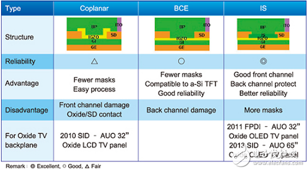
Common oxide thin film transistor device structure comparison table
The importance of oxide thin film transistor technology lies in the fact that its mass production model is compatible with the existing mainstream technology amorphous silicon equipment. The material characteristics of the oxide thin film transistor will change the electrical characteristics, that is, the critical voltage shift. (Threshold Voltage Shift, Vth Shift), even on Photo Sensors, so how to improve uniformity and reliability will be a big problem. The adjustment of the process is quite difficult and sensitive, and the process stability requirements are also required. Relatively high. Through continuous analysis and improvement with the laboratory, the researchers have developed a prototype circuit with a threshold voltage offset value of less than 0.8 volts on the oxide technology. After panel reliability testing, it is found that the service life estimate can exceed 10 years, which has surpassed the traditional amorphous silicon technology and is quite close to the low temperature polysilicon technology.
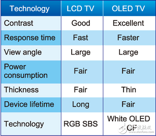
LCD and OLED characteristics comparison table
The OLED screen is composed of red, green and blue (R, G, B) pixels, which uses the mainstream organic material coating technology - vacuum evaporation, which is to balance the red, green and blue organic light in each pixel. The amount of body placement maintains the uniformity of brightness. As the size of the OLED screen increases, the yield of the product will decrease. Due to the short life of the blue organic illuminator, a little blue OLED will be evaporated a little in order to repair its defects. Organic illuminants, but the result is color distortion in red, green, and blue pixel configurations. In addition to the design of the vapor deposition tank, the production efficiency of the vapor deposition technology is not good, and it is also facing the difficult production environment of the vapor deposition equipment suitable for the 8th generation OLED panel production line. In addition to continuing to use the 5.5 generation line to produce OLED panels, you can also use laser technology for organic material coating, or use oxide panels and white OLEDs with color filters to filter out the red, blue, and green primary colors, closer to the current one. The liquid crystal display screen process, that is, the red, green and blue organic light-emitting bodies are vertically vapor-deposited on the whole white light OLED panel, and the color information is expressed by the color purification technology, and the uniform surface light source is obtained through the diffusion film after coating. Since the metal mask is not used when the organic material is vapor-deposited, it is not limited by the panel size, and the organic substance can be uniformly vapor-deposited, and the color is improved by vertically vaporizing the red, green, and blue organic light-emitting bodies, so the blue organic light-emitting The life of the body has been well solved. Although its color performance is relatively poor and consumes electricity, the yield is relatively high and it is easy to mass produce.
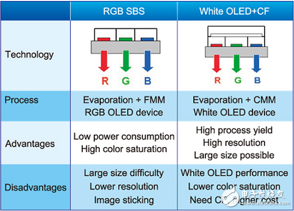
Common full color OLED technology comparison table
Common full-color OLED technologies mainly include red, green, and blue pixel juxtaposition (RGB-SBS, Side-By-Side) and white OLED + color filter (White OLED + Color Filter) technology. The red, green and blue pixel juxtaposition method consists of red, green and blue pixels respectively, which not only can obtain better color saturation, but also save power, but large-scale evaporation (EvaporaTIon) is not easy and needs continuous development.
Although the pixel technology of Fine Metal Mask (FMM, also called fine metal mask), which is relatively difficult to process, performs better in color performance and saves power, it immediately encounters challenges of large size, including challenges. Fine metal masking and color mixing requirements, as well as metal evaporation processes that challenge temperatures above 1000 °C. The researchers strictly implemented the process control, efficiently returned the process parameters, and with the Fine Divided Sheet (FDS) technology, finally succeeded in developing the non-mixing technology, achieving both the front-end oxide thin film transistor and the back-end OLED. A milestone in the production of Full Sheet.
Products with OLED curved screensSince the introduction of the Tandem OLED structure, high-efficiency white OLEDs have gradually come true, and with the technological evolution of materials and components, white OLED technology has reached an acceptable level in the field of lighting and display. However, compared to the wide color gamut and high color purity of OLEDs using red, green, and blue pixel juxtaposition methods, white OLED components are difficult to achieve. In addition, at least 10 layers of film are required to form a white light element. The thickness uniformity of the film on each OLED element over a long period of time is also a major problem to be solved in the metal evaporation apparatus.
Products with OLED large screenIn recent years, in addition to material evolution, the improvement of OLED component technology is a key to the success of the entire OLED industry. The optical weight thickness of the component is optimized, and the optimized optical thickness optimizes the color and luminous efficiency emitted by the organic light-emitting material, and the upper or lower light-emitting elements and the strong or weak resonant cavity are planned according to the properties of the product ( Cavity). The OLED device is designed to use a multilayer transmission layer and a novel blue luminescent material. Therefore, high efficiency and good blue chromaticity performance are obtained on the lower illuminating element of the weak resonant cavity, which is 83% under the CIE 1931 color coordinate. The performance of the color gamut, and the efficiency of the component, due to the application of the multi-transport layer, significantly enhances the energy recovery on the triplet level of the fluorescent light-emitting layer material, thereby improving the performance of the component. In addition, the OLED component is equipped with an OLED pixel compensation circuit (OLED Engine), which can effectively improve the brightness unevenness caused by the threshold voltage shift of the oxide thin film transistor and the OLED.
In order to achieve a thinner and lower cost OLED screen, the traditional glass packaging technology should be replaced by a mass-produced thin film packaging technology. The OLED screen is combined with the upper and lower panels. In the traditional process, the upper panel is generally made of glass, but the thin film packaging technology that is light in weight, thin and low-cost is the trend. Since the process temperature of the low-temperature polycrystalline germanium panel is as high as 600 ° C, the high temperature resistance of the glass panel is not good, and therefore, the heat resistance of the OLED glass panel is bound by technology. In order to improve the yield of low-temperature polycrystalline germanium panel process and shorten the mass production time of OLED screen, OLED glass panel companies produce Lotus Glass, which has zero impurity and high flatness, which is suitable for low-temperature polycrystalline high-temperature process. The characteristics of heat resistance stability are supplied to some existing 4.5 and 5.5 generation OLED panel production lines.
At present, organic optoelectronics still has a series of theoretical, technical and technological problems in terms of materials, efficacy, life, colorization, large size, flexibility, packaging and production processes. The defects in these links are constrained to a considerable extent. The development of organic photoelectric functional materials and technologies in the direction of industrialization. Among them, OLED technology to achieve large-scale applications, depending on the overall progress of materials, design and preparation processes, but also need to innovate materials and device structures to improve efficiency, increase stability and reduce costs.
Note: Vacuum evaporation - the technology of depositing organic materials in a crucible under vacuum to evaporate and deposit a film on a glass substrate covered with a mask (MASK) is currently the most mature and At present, the mass-produced small-size active-drive (AMOLED) products basically adopt organic film-forming technology, but the fine metal mask pixel technology has high alignment precision requirements for the mask and the glass substrate, and the mask is affected by gravity and Thermal expansion is easy to deform, and the material utilization rate is low.
Editor's conclusionApple said it will use OLED screens on the iPhone 8 this year, and its demonstration effect in the field of electronic products such as smart phones will be an important driving force for OLED. With the explosion of new electronic products such as VR (virtual reality) and wearable devices, OLED will bring new entry points. The market for OLED terminal products has exploded rapidly, which will drive the growth prospects of OLEDs. In general, this year is likely to become the “first year of OLEDâ€.
Wall-mounted Energy Storage Lithium Battery
Enershare's commitment to future-ready energy solutions for smart home innovations, Enershare's Energy Storage Systems create a flexible energy maintenance system for homeowners who want to take more control of their home energy use, it is intended to be used for home battery energy storage and stores electricity for solar self-consumption, load shifting, backup power, and off-the-grid use. you can use it anytime you want-at night or during an outage.
Solar Battery Bank,Solar Energy Storage,Solar House Battery,Solar Battery Storage,Lithium Battery Off Grid,Solar Battery Backup 48v
Shenzhen Enershare Technology Co.,Ltd , https://www.enersharepower.com